Bit scan circuits and method in non-volatile memory

a non-volatile memory and bit scan technology, applied in the field of electronic circuits and methods, can solve the problems of unsuitable mobile and handheld environment, prone to mechanical failure, bulky disk drives, etc., and achieve the effect of simplifying circuits, improving the failure bit counting speed, and reducing layout siz

Inactive Publication Date: 2013-04-23
SANDISK TECH LLC
View PDF18 Cites 7 Cited by
  • Summary
  • Abstract
  • Description
  • Claims
  • Application Information

AI Technical Summary

Benefits of technology

[0015]In a more preferred embodiment, M is determined from the number of the missing pulses which is counted from a branch of the clock signal that does not passes through the daisy chain. The branch of the clock signal is gated outside the daisy chain to minimize gate delays suffered through the entire daisy chain. The gating signal is provided by the tag bits from the individual tag latches of the daisy chain.
[0019]This invention substantially improves failure bits counting speed, employs relatively simplified circuits, thereby reducing layout size and reducing power consumption. In general, it can be used for bit count in memory products and achieving the operation with fast operation and small circuit area.

Problems solved by technology

Conventional mass storage, based on rotating magnetic medium such as hard drives and floppy disks, is unsuitable for the mobile and handheld environment.
This is because disk drives tend to be bulky, are prone to mechanical failure and have high latency and high power requirements.
These undesirable attributes make disk-based storage impractical in most mobile and portable applications.
Obviously, the more bits a memory cell is configured to store, the smaller is the margin of error it has to operate in.
Existing circuits and methods to scan this string for occurrence of “1”s can be time and / or hardware intensive.

Method used


Image

  • Bit scan circuits and method in non-volatile memory
  • Bit scan circuits and method in non-volatile memory
  • Bit scan circuits and method in non-volatile memory

Examples


Embodiment Construction

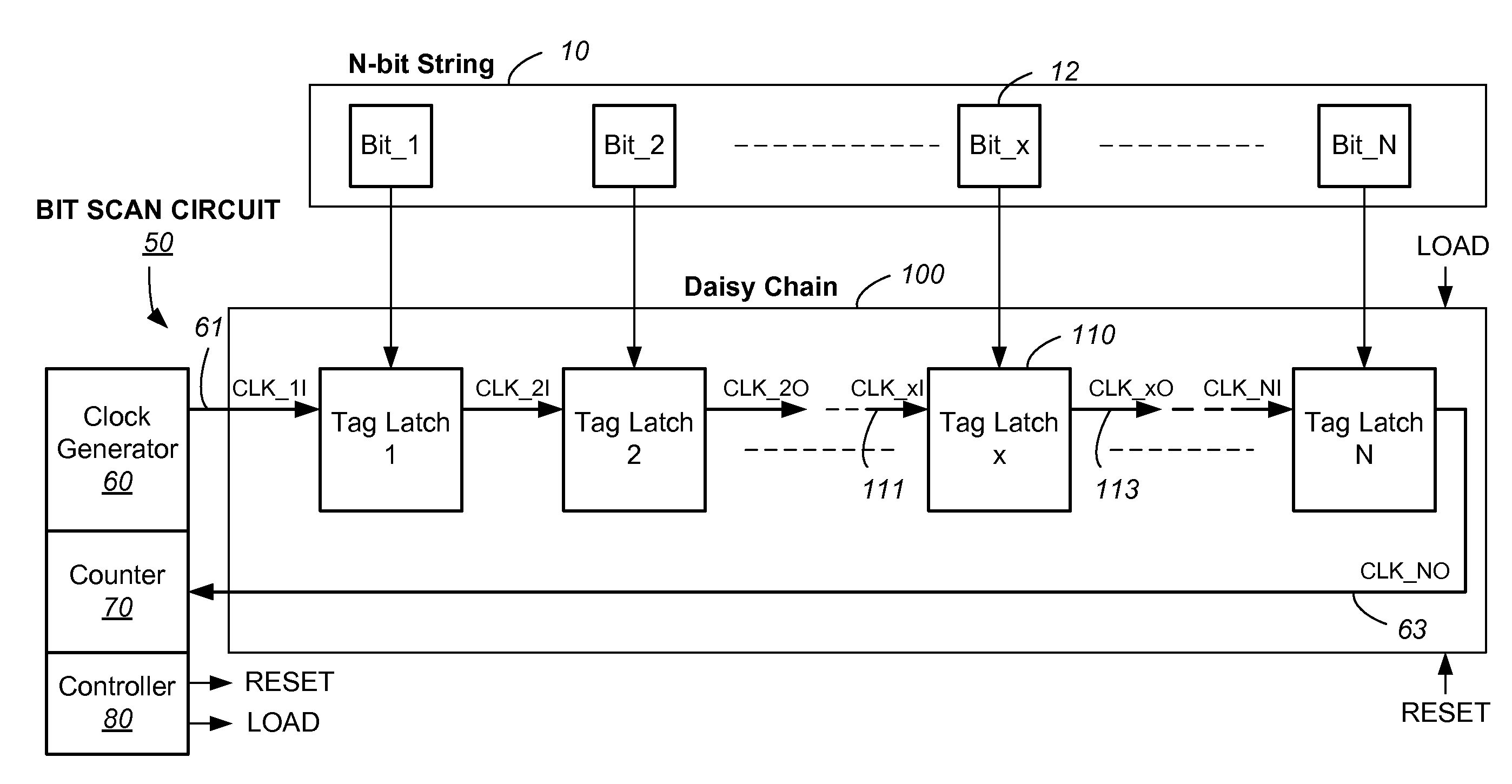
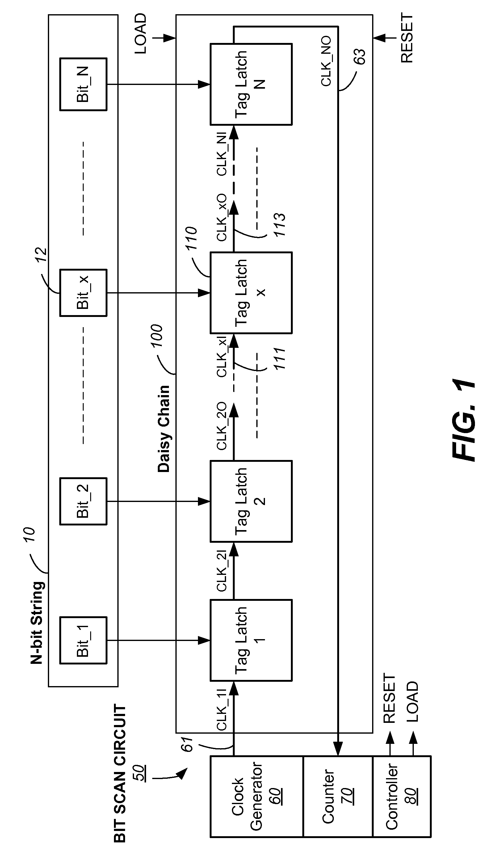
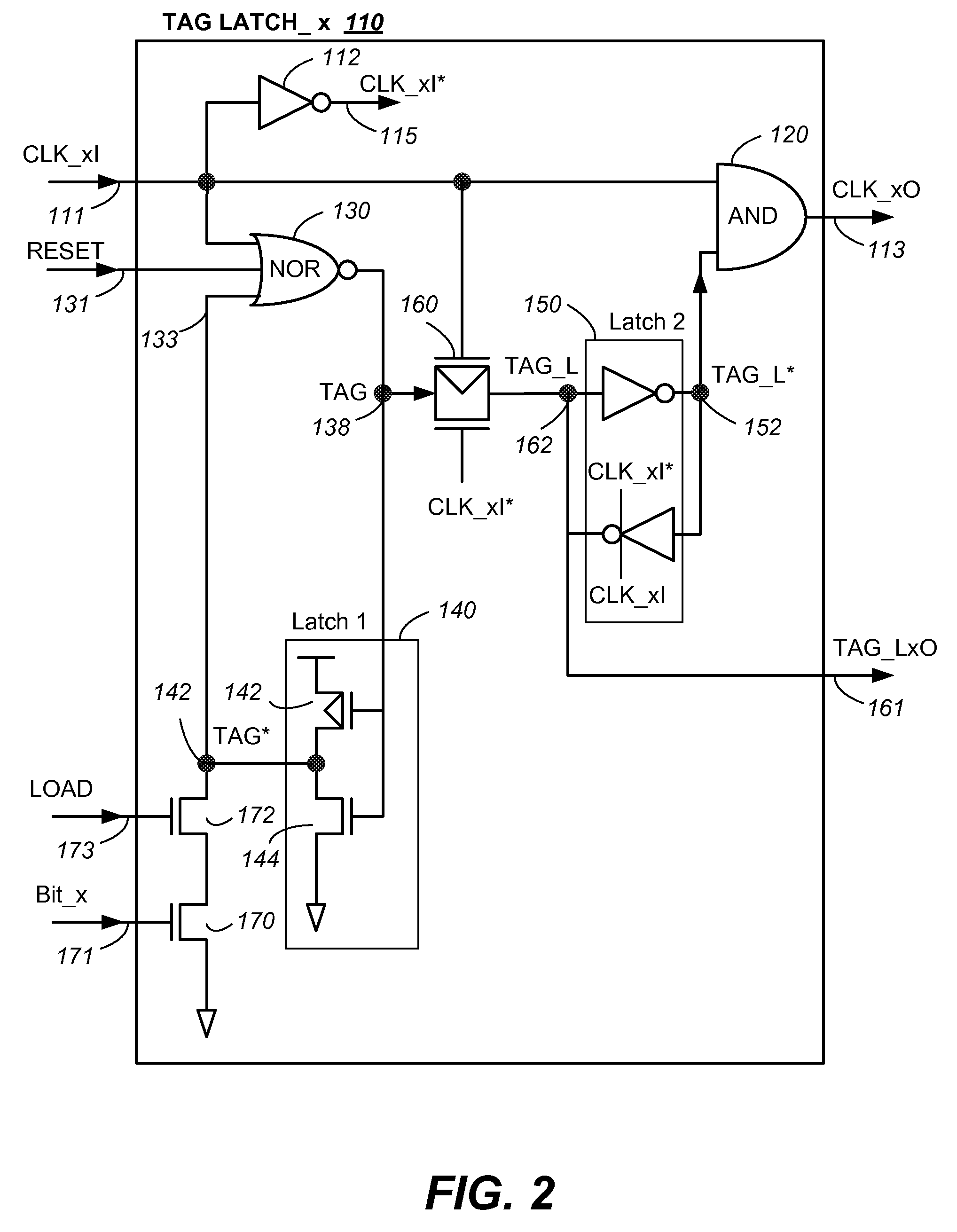
[0032]FIG. 1 illustrates a bit scan circuit according to one embodiment of the invention in which a gated clock signal is routed through a daisy chain of tag latches. The bit scan circuit 50 is employed to scan the number of “1”s and / or “0”s in an N-bit string 10. The bit scan circuit comprises N tag latches such as tag latch_1, tag latch_2, . . . , tag latch_x 110, . . . , tag latch_N. Each tag latch, such as tag latch_x 110 has a clock input CLK_xI 111 and a clock output CLK_xO 113. A daisy chain 100 is formed with the N tag latches daisy-chained together by their clock inputs and clock outputs.

[0033]The daisy chain 100 has an input end 61 which is the clock input of the first tag latch_1 and an output end 63 which is the clock output of tag latch_N. A clock generator 60 generates a clock signal CLK_1I which is input to the tag latch daisy chain 100 via the input end 61. The output end 63 of the daisy chain outputs a clock signal CLK_NO, which is fed back to a counter 70.

[0034]As ...


PUM


Abstract

A circuit for counting in an N-bit string a number of bits M, having a first binary value includes N latch circuits in a daisy chain where each latch circuit has a tag bit that controls each to be either in a no-pass or pass state. Initially the tag bits are set according to the bits of the N-bit string where the first binary value corresponds to a no-pass state. A clock signal having a pulse train is run through the daisy chain to “interrogate” any no-pass latch circuits. It races right through any pass latch circuit. However, for a no-pass latch circuit, a leading pulse while being blocked also resets after a pulse period the tag bit from “no-pass” to “pass” state to allow subsequent pulses to pass. After all no-pass latch circuits have been reset, M is given by the number of missing pulses from the pulse train.

Description

FIELD OF THE INVENTION[0001]This application relates generally to electronic circuits and methods and more particularly, to a circuit and method for counting the number of “1” or “0” in an N-bit string useful in the operation of re-programmable non-volatile memory systems such as semiconductor flash memory.BACKGROUND OF THE INVENTION[0002]Solid-state memory capable of nonvolatile storage of charge, particularly in the form of EEPROM and flash EEPROM packaged as a small form factor card, has recently become the storage of choice in a variety of mobile and handheld devices, notably information appliances and consumer electronics products. Unlike RAM (random access memory) that is also solid-state memory, flash memory is non-volatile, and retaining its stored data even after power is turned off. Also, unlike ROM (read only memory), flash memory is rewritable similar to a disk storage device. In spite of the higher cost, flash memory is increasingly being used in mass storage applicatio...

Claims


Application Information

Patent Timeline
Patent Type & Authority Patents(United States)
IPC IPC(8): G11C7/10
CPCG11C29/44G11C29/40
Inventor LIU, BOPARK, JONGMINCHEN, CHENKUO, TIEN-CHIEN
Owner SANDISK TECH LLC
Why Eureka
Try Eureka