System-on-chip with memory speed control core

a technology of memory speed control and system on-chip, applied in pulse generators, instruments, pulse techniques, etc., can solve the problems of reducing the number, increasing the complexity of ddr memory controllers, and increasing the difficulty of adding more channels, so as to improve the power efficiency rate, speed parameters of memory controller ram can be modified, and memory can be slowed.

Active Publication Date: 2013-05-07
MACOM CONNECTIVITY SOLUTIONS LLC
View PDF2 Cites 13 Cited by
  • Summary
  • Abstract
  • Description
  • Claims
  • Application Information

AI Technical Summary

Benefits of technology

[0016]Described herein are a system and method to change the speed of a memory controller (and memory) on-the-fly. This technique can be used in conjunction with the thermal management of a double data rate (DDR) memory, for example. In the event of overheating, a system-on-chip (SoC) thermal management core can instruct the DDR Controller to change the speed of the DDR Memory, to reduce the dual in-line memory module (DIMM) temperature or the DIMM Ambient Temperature. Further, the technique can be used for a power saving mode, when maximum performance is permitted by the thermal conditions, but is not required. For instance, if the central processing unit (CPU) core is slowed, the memory can be slowed down as well, to a more power efficient rate, still sufficient to support the CPU. Advantageously, the speed parameters of the memory controller RAM can be modified, to support different memory speeds, without resetting the system and without losing the data in the RAM. No data is lost since the RAM is put in self-refresh mode before changing the RAM speed.

Problems solved by technology

DDR memory controllers are significantly more complicated than Single Data Rate controllers, but allow for twice the data to be transferred without increasing the clock rate or increasing the bus width to the memory cell.
In theory, more channels can be built (a channel for every DRAM cell would be the ideal solution), but due to wire count, line capacitance, and the need for parallel access lines to have identical lengths, more channels are very difficult to add.
This decreases the number of the wires necessary to place the memory devices on a motherboard (allowing for a smaller number of layers to be used, meaning more memory devices can be placed on a single board), at the expense of increasing latency (the time necessary to access a memory location).
In theory, the FB-DIMM's memory buffer device could be built to access any DRAM cells, allowing for memory cell agnostic memory controller design, but this has not been demonstrated, as the technology is in its infancy.
Changing memory parameters while the system is running requires many factors to be taken into account and, requires specialized logic that adds to the cost of the chips.
Given that low cost is a key selling factor, and that battery life and power efficiency are less so, means that such functionality has not been addressed before.
Changing the memory hardware timing on-the-fly can lead to complications, such as memory corruption, microprocessor hang ups due to glitches and loss of state.

Method used


Image

  • System-on-chip with memory speed control core
  • System-on-chip with memory speed control core
  • System-on-chip with memory speed control core

Examples


Embodiment Construction

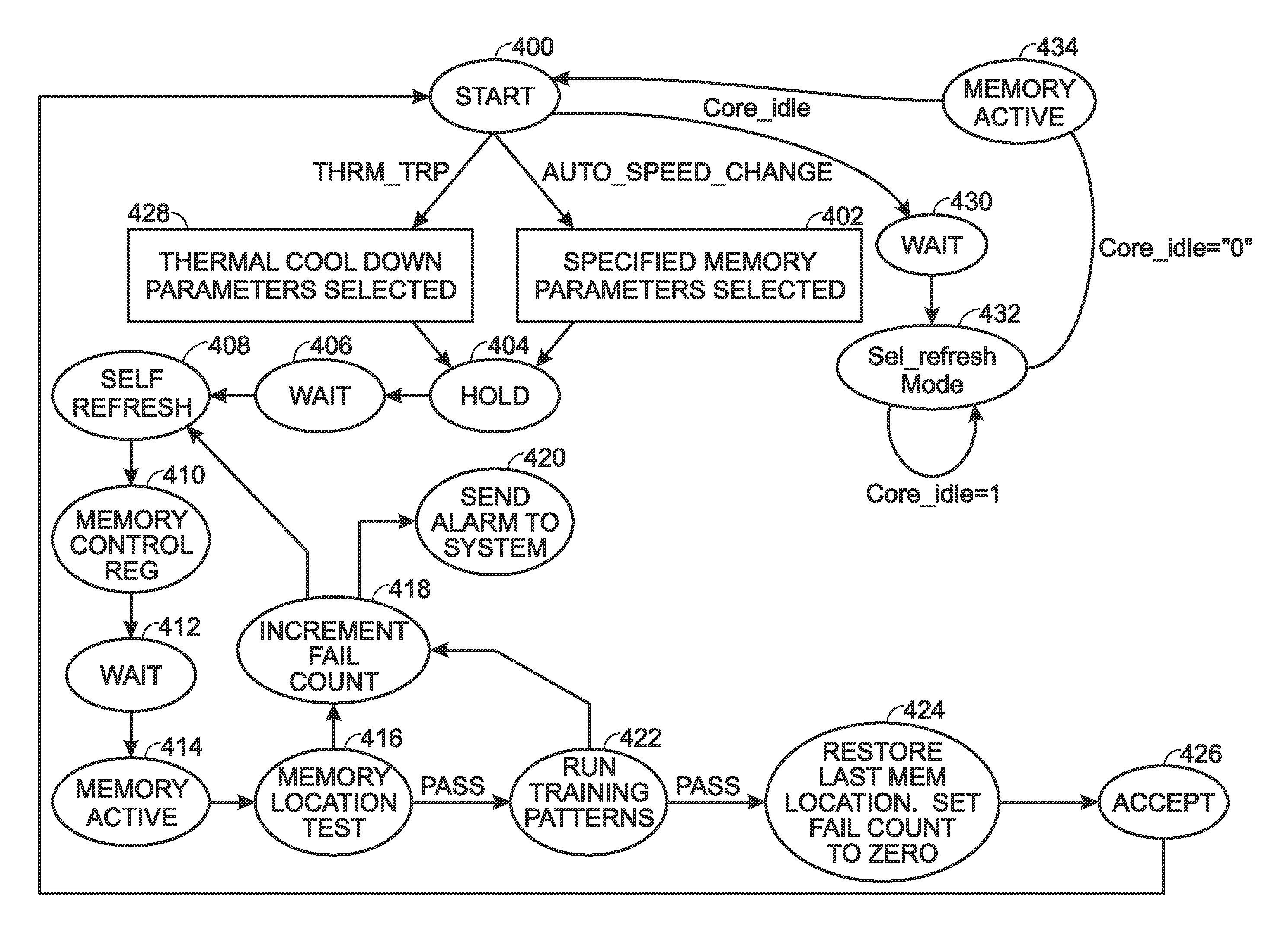
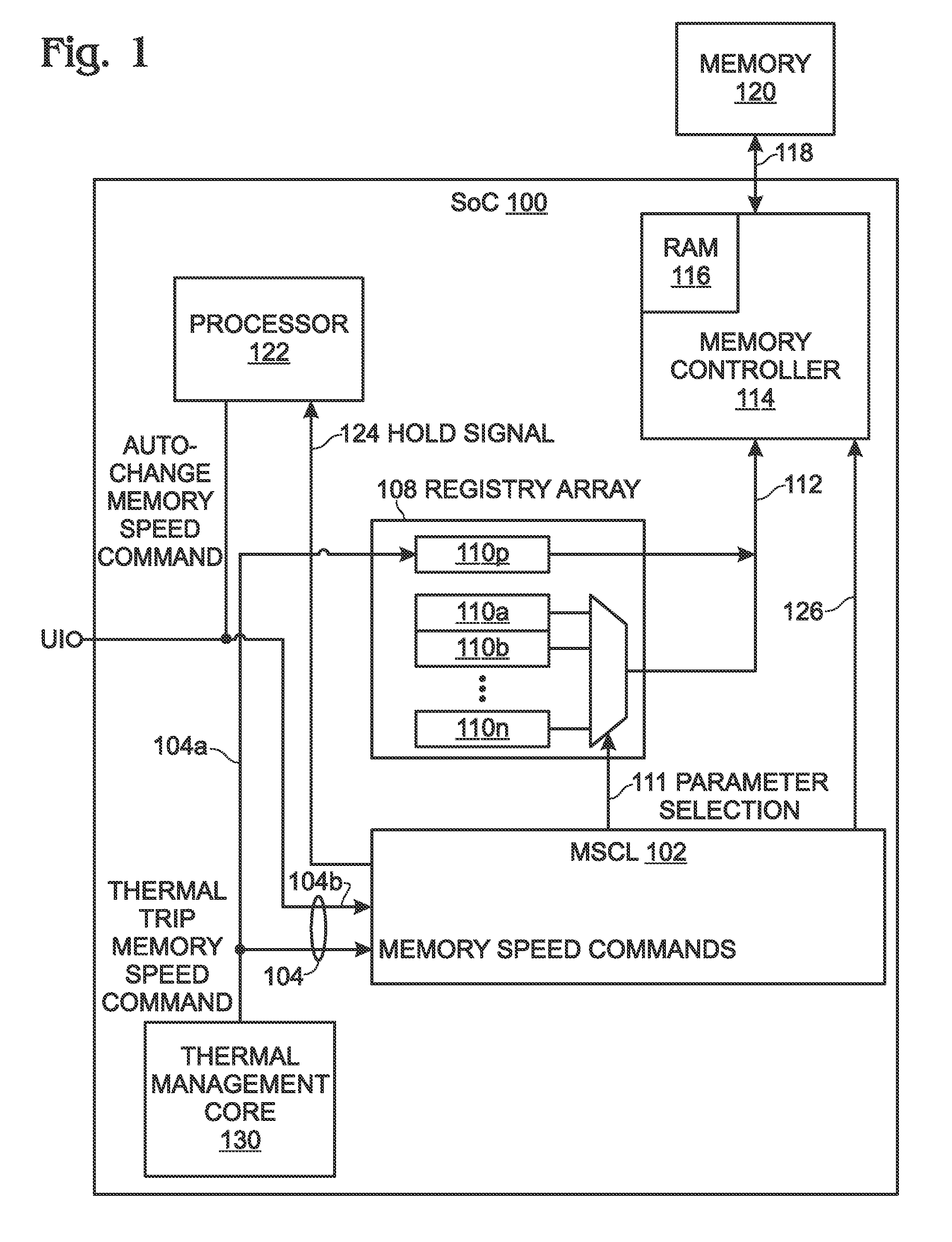
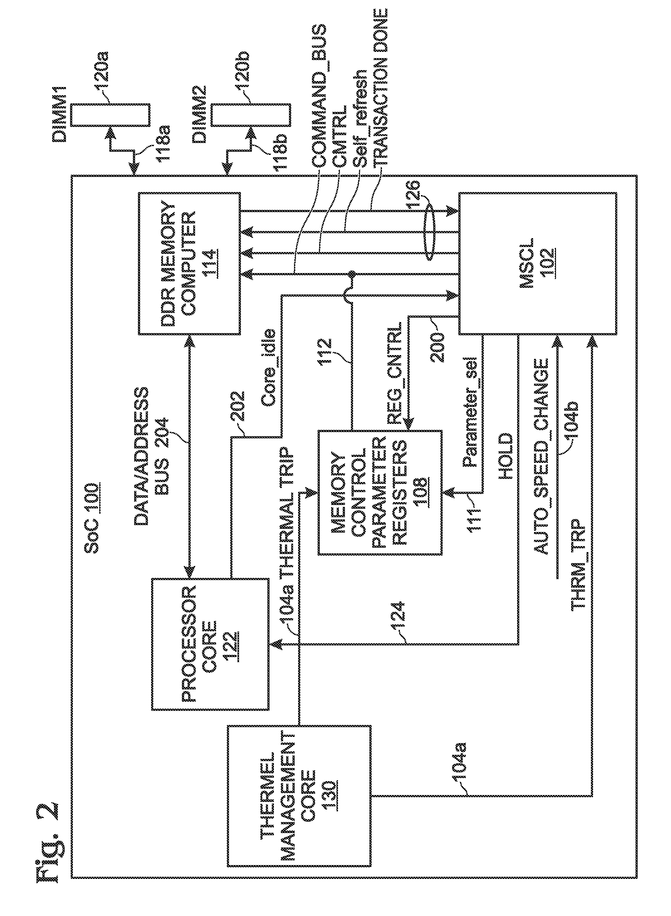
[0026]FIG. 1 is a schematic block diagram of a system-on-chip (SoC) with memory speed control logic to control memory maintenance and access parameters. The SoC 100 comprises an internal hardware-enabled memory speed control logic (MSCL) core 102 having an interface on line 104 to accept memory speed commands and an interface on line 106 to supply parameter select commands. The SoC 100 includes an array 108 of memory control parameter registers 110 having an interface on line 111 to supply a selected a set of parameters from one of the registers 110. Shown are registers 110a through 110n, where n is a variable not limited to any particular value. A memory controller 114 has an interface on line 112 to accept the selected set of parameters from the register array 108, to replace an initial set of parameters in RAM 116. The memory controller 114 has an interface on line 118 connected to an off-SoC memory 120. The memory controller 114 manages the off-SoC memory 120 using the set of pa...


PUM


Abstract

A system and method are provided for using a system-on-chip (SoC) memory speed control logic core to control memory maintenance and access parameters. A SoC is provided with an internal hardware-enabled memory speed control logic (MSCL) core. An array of SoC memory control parameter registers is accessed and a set of parameters is selected from one of the registers. The selected set of parameters is delivered to a SoC memory controller, to replace an initial set of parameters, and the memory controller manages an off-SoC memory using the delivered set of parameters.

Description

RELATED APPLICATIONS[0001]This application is a Continuation-in-Part of a pending application entitled, SYSTEM-ON-CHIP WITH THERMAL MANAGEMENT CORE, invented by Waseem Kraipak et al., Ser. No. 12 / 687,817, filed Jan. 14, 2010;[0002]which is a Continuation-in-Part of a pending application entitled, SYSTEM-ON-CHIP WITH FEEDBACK LOOP FOR PROCESSOR FREQUENCY CONTROL, invented by Waseem Kraipak et al., Ser. No. 12 / 639,064, filed Dec. 16, 2009. Both these applications are incorporated herein by reference.BACKGROUND OF THE INVENTION[0003]1. Field of the Invention[0004]This invention generally relates to system-on-chip (SoC) off-SoC memory management and, more particularly, to a system and method for using a SoC hardware core to control the frequency of memory operations.[0005]2. Description of the Related Art[0006]As noted in Wikipedia, a memory controller is a digital circuit that manages the flow of data going to and from the main memory. The memory controller can be a separate chip or in...

Claims


Application Information

Patent Timeline
Patent Type & Authority Patents(United States)
IPC IPC(8): G06F12/00G06F13/00G06F13/28G06F11/00G11C29/00G11C7/04G11C11/34H01L35/00H01L37/00G06F1/00G06F1/32
CPCG06F1/206G06F1/3225G06F1/3275G11C7/04G11C11/40615G11C11/40626G11C29/56G11C2029/0401G11C2207/2254Y02D10/00
Inventor KRAIPAK, WASEEM SAIFYBENDAK, GEORGE
Owner MACOM CONNECTIVITY SOLUTIONS LLC
Why Eureka
Try Eureka