Methods and materials for fabricating microfluidic devices

a microfluidic device and microfluidic technology, applied in microstructural devices, microstructural technology, polyether coatings, etc., can solve the problems of microfluidic applications that require clean-room conditions, photolithography and etching techniques are expensive and labor-intensive, and pdms suffers from multiple drawbacks, etc., to achieve low surface energy

Active Publication Date: 2013-05-21
THE UNIV OF NORTH CAROLINA AT CHAPEL HILL
View PDF132 Cites 34 Cited by
  • Summary
  • Abstract
  • Description
  • Claims
  • Application Information

AI Technical Summary

Benefits of technology

[0090]According to some embodiments, a method of increasing chemical compatibility of a polymeric device includes treating a polymeric device comprising a latent methacrylate, acrylate, and / or styrene group with a solution comprising a styrene end-capped precursor solution, evaporating or dissolving the solution such that a film of the styrene end-capped precursor remains on a surface of the polymeric device, and curing the styrene end-capped precursor film such that the film adheres to the surface of the polymeric device through reaction with latent methacrylate, acrylate, and / or styrene groups of the polymeric device.

Problems solved by technology

Photolithography and etching techniques, however, are costly and labor intensive, require clean-room conditions, and pose several disadvantages from a materials standpoint.
The increasing complexity of microfluidic devices has created a demand to use such devices in a rapidly growing number of applications.
Despite the aforementioned advantages, PDMS suffers from multiple drawbacks in microfluidic applications.
First, PDMS swells in most organic solvents.
Thus, PDMS-based microfluidic devices have a limited compatibility with various organic solvents.
The swelling of a PDMS microfluidic device by organic solvents can disrupt its micron-scale features, e.g., a channel or plurality of channels, and can restrict or completely shut off the flow of organic solvents through the channels.
Thus, microfluidic applications with a PDMS-based device are limited to the use of fluids, such as water, that do not swell PDMS.
This approach, however, is limited by the disadvantages of fabricating microfluidic devices from hard materials.
Second, PDMS-based devices and materials are notorious for not being adequately inert to be used even in aqueous-based chemistries.
For example, PDMS is susceptible to reaction with weak and strong acids and bases.
PDMS-based devices also are notorious for containing extractables, such as extractable oligomers and cyclic siloxanes, especially after exposure to acids and bases.
In Rolland, J. et al., supra, multilayer PFPE devices were generated using a specific partial UV curing technique, however, the adhesion was weak and generally not strong enough for a wide range of microfluidic applications.
Further, the adhesion technique described by Rolland, J. et al. did not provide for adhesion to other substrates such as glass.
Further, adequate adhesion between the layers of a multilayer microfluidic device can impact performance in most if not all applications.
Although these and other materials commonly used as implant materials have proven to be useful there are many drawbacks with the materials.
One drawback is that with any implant there is always the chance of bio-fouling on the surface of the implant.
Bio-fouling can occur due to the tissue / implant interface gap and the surface characteristics of the implant material.

Method used


Image

  • Methods and materials for fabricating microfluidic devices
  • Methods and materials for fabricating microfluidic devices
  • Methods and materials for fabricating microfluidic devices

Examples


example 1

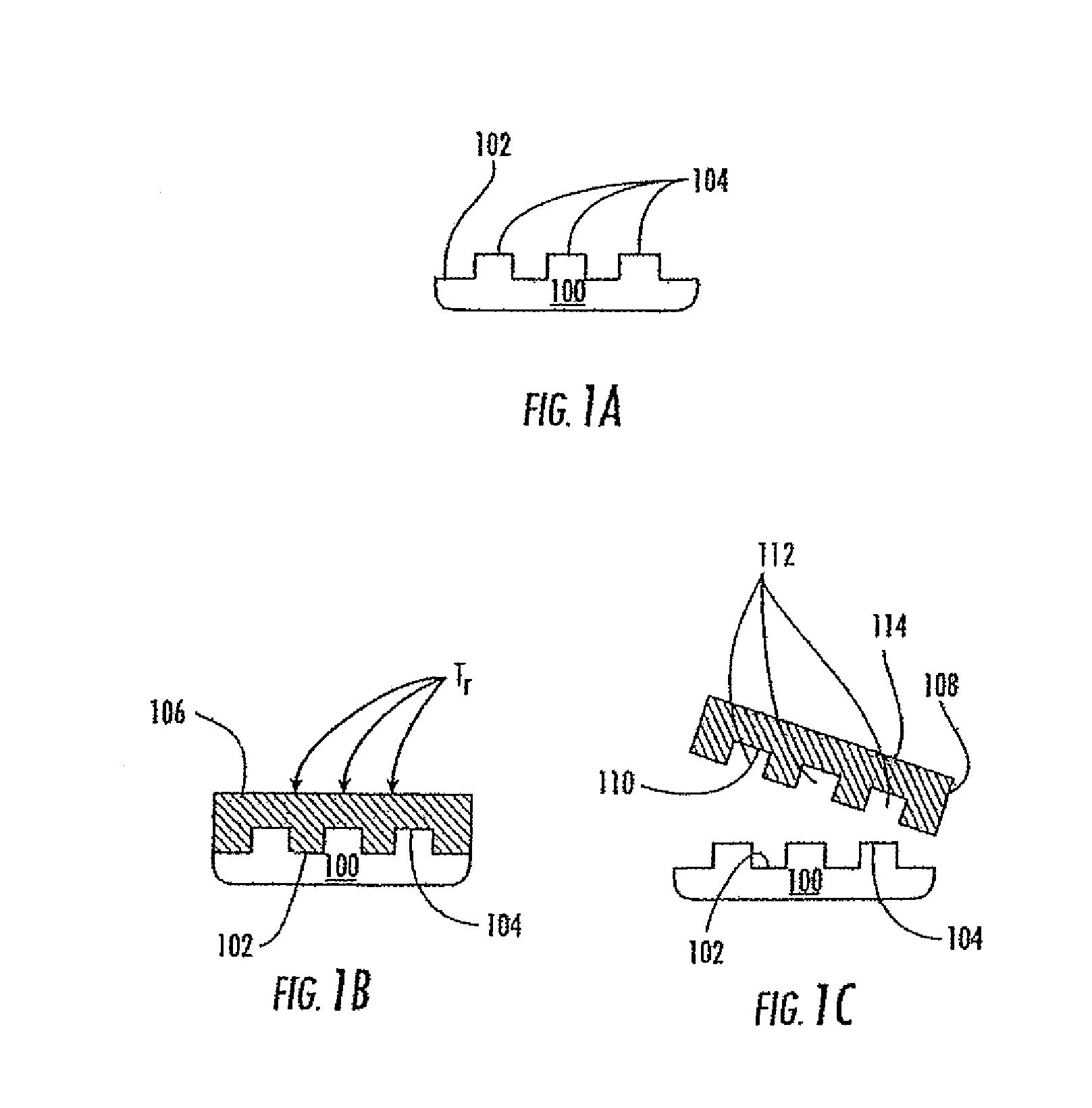
[0657]A liquid PFPE precursor having the structure shown below (where n=2) is blended with 1 wt % of a free radical photoinitiator and poured over a microfluidics master containing 100-μm features in the shape of channels. A PDMS mold is used to contain the liquid in the desired area to a thickness of about 3 mm. The wafer is then placed in a UV chamber and exposed to UV light (λ=365) for 10 minutes under a nitrogen purge. Separately, a second master containing 100-μm features in the shape of channels is spin coated with a small drop of the liquid PFPE precursor over top of it at 3700 rpm for 1 minute to a thickness of about 20 μm. The wafer is then placed in a UV chamber and exposed to UV light (λ=365) for 10 minutes under a nitrogen purge. Thirdly, a smooth, flat PFPE layer is generated by drawing a doctor's blade across a small drop of the liquid PFPE precursor across a glass slide. The Slide is then placed in a UV chamber and exposed to UV light (λ=365) for 10 minutes under a ni...

example 2

Thermal Free Radical

Glass

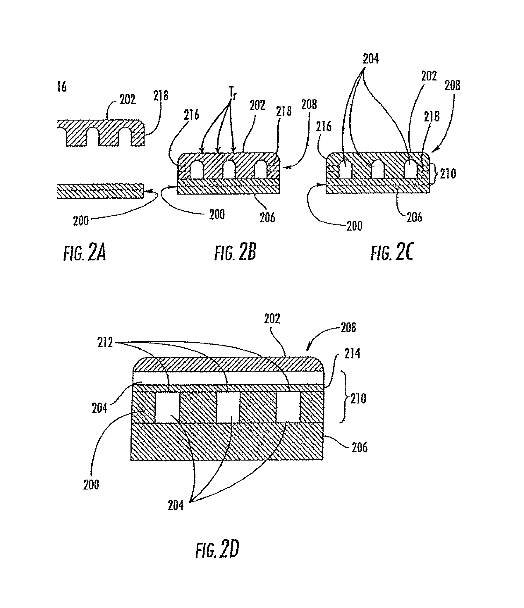
[0659]A liquid PFPE precursor encapped with methacrylate groups is blended with 1 wt % of 2,2-Azobisisobutyronitrile and poured over a microfluidics master containing 100-μm features in the shape of channels. A PDMS mold is used to contain the liquid in the desired area to a thickness of about 3 mm. The wafer is then placed in an oven at 65° C. for 20 hours under nitrogen purge. The cured layer is then removed, trimmed, and inlet holes are punched through it using a luer stub. The layer is then placed on top of a clean glass slide and fluids can be introduced through the inlet holes.

example 3

Thermal Free Radical

Partial Cure

Layer to Layer Adhesion

[0660]A liquid PFPE precursor encapped with methacrylate groups is blended with 1 wt % of 2,2-Azobisisobutyronitrile and poured over a microfluidics master containing 100-μm features in the shape of channels. A PDMS mold is used to contain the liquid in the desired area to a thickness of about 3 mm. The wafer is then placed in an oven at 65° C. for 2-3 hours under nitrogen purge. Separately, a second master containing 100-μm features in the shape of channels is spin coated with a small drop of the liquid PFPE precursor over top of it at 3700 rpm for 1 minute to a thickness of about 20 μm. The wafer is then placed in an oven at 65° C. for 2-3 hours under nitrogen purge. Thirdly, a smooth, flat PFPE layer is generated by drawing a doctor's blade across a small drop of the liquid PFPE precursor across a glass slide. The wafer is then placed in an oven at 65° C. for 2-3 hours under nitrogen purge. The thicker layer is then removed, ...


PUM

PropertyMeasurementUnit
Young's modulusaaaaaaaaaa
surface energyaaaaaaaaaa
elongation at breakaaaaaaaaaa

Abstract

Materials and Methods are provided for fabricating microfluidic devices. The materials include low surface energy fluoropolymer compositions having multiple cure functional groups. The materials can include multiple photocurable and / or thermal-curable functional groups such that laminate devices can be fabricated. The materials also substantially do not swell in the presence of hydrocarbon solvents.

Description

CROSS REFERENCE TO RELATED APPLICATIONS[0001]This application is a divisional of U.S. application Ser. No. 12 / 063,284, filed May 29, 2009 now U.S. Pat. No. 8,158,728, which is a U.S. national stage application of PCT / US06 / 031607, filed Aug. 9, 2006, which claims the benefit of U.S. Provisional Patent Application Ser. No. 60 / 706,786, filed Aug. 9, 2005; U.S. Provisional Patent Application Ser. No. 60 / 732,727, filed Nov. 2, 2005; and U.S. Provisional Patent Application Ser. No. 60 / 799,317 filed May 10, 2006; each of which is incorporated herein by reference in its entirety.[0002]This application is also based on a Continuation in part of PCT International Patent Application Serial No. PCT / US05 / 04421, filed Feb. 14, 2005, which is based on and claims priority to U.S. Provisional Patent Application Ser. No. 60 / 544,905, filed Feb. 13, 2004, each of which is incorporated herein by reference in its entirety.FEDERALLY SPONSORED RESEARCH OR DEVELOPMENT[0003]This invention was made with U.S. ...

Claims


Application Information

Patent Timeline
Patent Type & Authority Patents(United States)
IPC IPC(8): B29C33/40
CPCC08G18/8175B29C66/9534B29C66/919B29C66/91431B29C66/949B01L3/502707B29C33/3878B29C33/405B29C66/54B29C66/71B81C99/0085C08G18/10C08G18/5015B29C66/727C08G59/30C08L71/02C08L75/16B29C59/005B29C66/543B29C65/48C08G18/50B29C65/00B29C65/485B01L2300/0887B01L2300/12B29C65/4845B29C65/521B29K2883/00B29L2031/756B81B2201/051B29C65/4835C08G65/007B29C66/723B29L2031/7172Y10T137/0318Y10T137/2224C09D171/00B29K2027/18B29K2027/12
Inventor DESIMONE, JOSEPH M.ROLLAND, JASON P.ROTHROCK, GINGER M. DENISONRESNICK, PAUL
Owner THE UNIV OF NORTH CAROLINA AT CHAPEL HILL
Why Eureka
Try Eureka