Method of manufacturing a laser diode with improved light-emitting characteristics

a laser diode and performance characteristic technology, applied in the direction of lasers, instruments, electrical equipment, etc., can solve the problems of insufficient radiation quality of edge-emitting laser diodes, complicated light beams emitted from aforementioned edge-emitting laser diodes, and complicated light beam structure of slow-axis beams, etc., to achieve high power, reduce angular divergence in the direction of slow axis, and high thermal conductivity

Inactive Publication Date: 2013-05-28
OOO NANOOPTIC DEVICES
View PDF13 Cites 14 Cited by
  • Summary
  • Abstract
  • Description
  • Claims
  • Application Information

AI Technical Summary

Problems solved by technology

One of the problems that currently exists in the field of laser technology is insufficient quality of radiation from edge-emitting laser diodes.
It is known that light beams emitted from aforementioned edge-emitting laser diodes have a complicated structure.
On the other hand, the slow-axis beam structure can be very complicated, and collimation is very difficult, if even possible.
The radiation structure of the aforementioned type significantly complicates formation of desired beams and their collimation and focusing on a target, as well as coupling into optical fibers.
However, precision collimators of this type are expensive, and this limits their use in practice.
The output power of these diodes exceeds several watts and may reach tens of watts, and the structure of their radiation has a complicated multimode nature that leads to high divergence of the output beam.
Conventional approaches to the solution of the above problem with respect to the wide-aperture edge-emitting laser diodes do not allow for forming single transverse mode beams without significant loss of power and with increase in weight or size.
Therefore, advantages inherent in optical laser devices are not used to their full potentials for wide-aperture edge-emitting laser diodes.

Method used


Image

  • Method of manufacturing a laser diode with improved light-emitting characteristics
  • Method of manufacturing a laser diode with improved light-emitting characteristics
  • Method of manufacturing a laser diode with improved light-emitting characteristics

Examples


Embodiment Construction

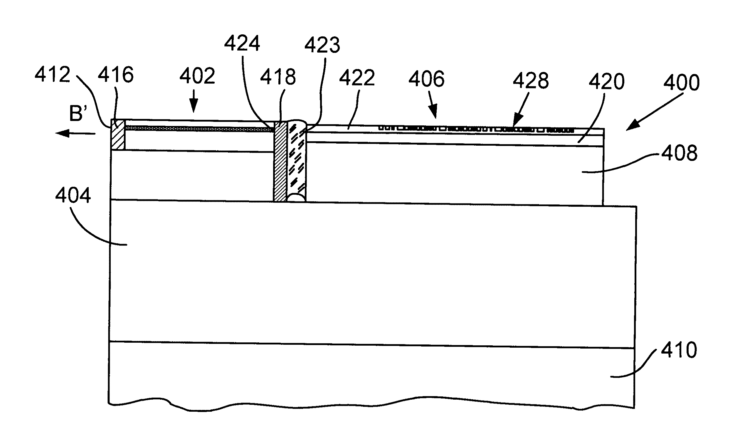
[0039]Terminology used in the present specification is explained below. In the context of the present patent specification, the term “lasing medium” relates to a part of a laser-type light-emitting device, such as a laser diode, that forms the aforementioned device in combination with respective fully reflecting and / or partially reflecting mirrors.

[0040]Furthermore, although mode structures are considered in general, all modifications described below relate to lateral modes. Some important properties of laser diodes depend on the geometry of the optical cavity. Thus, in the vertical direction, light is contained in a very thin layer, and, therefore, in the direction perpendicular to the layers the structure supports only a single optical mode. In the lateral direction, however, if the waveguide is wide in comparison to the wavelength of light, the waveguide can support multiple lateral optical modes. In the latter case, such a laser is known as “multimode laser.”

[0041]For better und...


PUM


Abstract

The method of the invention is intended for manufacturing a laser diode with improved light-emitting characteristics. The method consists of providing certain components of a laser diode such as a wide-aperture lasing medium that has an active emitting layer with a first end and a second end, a DPH-mode reorganizer that contains a core and a plurality of nanogrooves made in the core and arranged in a pattern that accomplishes a given function and locally changes the refractive index of the core. The method further includes the steps of forming a semitransparent mirror on the second end of the active lasing medium and aligning the first end of the active emitting layer with the core of the DPH-mode reorganizer, thus forming a resonator of the laser diode. In the resonator, the light applied from the laser-active medium bounces back and forth between the DPH-mode reorganizer and the partially reflecting mirror, thereby enhancing stimulated emission.

Description

CROSS-REFERENCE TO RELATED PATENT DOCUMENTS[0001]The present patent application is continuation-in-part of U.S. patent application Ser. No. 12 / 592,191 filed by the same applicant on Nov. 23, 2009 now U.S. Pat. No. 8,085,821 and entitled “Light-Enhancing Device and Method Based on Use of an Optically Active Lasing Medium in Combination with Digital Planar Holography”.FIELD OF THE INVENTION[0002]The present invention relates to a method of manufacturing a laser device, in particular, to manufacturing a laser device with improved performance characteristics. More specifically, the invention relates to a method for manufacturing a laser diode based on a broad area cavity design and on the use of digital planar holography. The invention may be used for enhancing brightness of light produced by a device based on the use of laser diodes in combination with digital planar holograms. The aforementioned method uses a multimode laser diode in combination with a digital planar hologram and redu...

Claims


Application Information

Patent Timeline
Patent Type & Authority Patents(United States)
IPC IPC(8): H01S3/098
CPCG02B5/32G02B6/124G02B6/4202G03H1/0408H01S5/141H01S3/08031H01S3/08045H01S5/02248H01S5/2036H01S5/02325
Inventor YANKOV, VLADIMIR
Owner OOO NANOOPTIC DEVICES
Why Eureka
Try Eureka