Semiconductor device and method for manufacturing the same
a semiconductor and on-current technology, applied in semiconductor devices, instruments, electrical equipment, etc., can solve the problems of insufficient ratio of on-current to off-current, change in transistor characteristics such as threshold values, etc., and achieve excellent productivity and higher reliability.
- Summary
- Abstract
- Description
- Claims
- Application Information
AI Technical Summary
Benefits of technology
Problems solved by technology
Method used
Image
Examples
embodiment 1
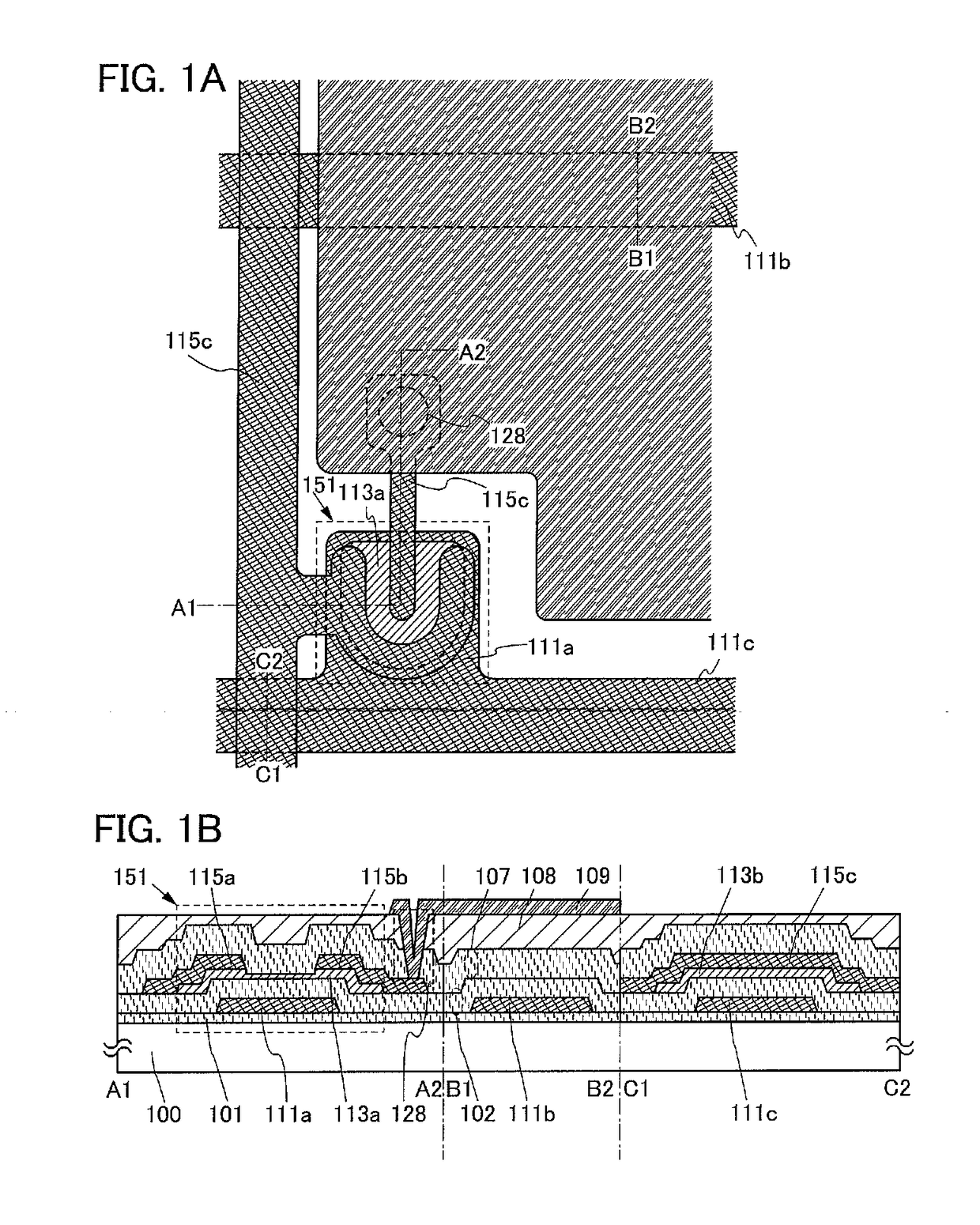
[0090]In this embodiment, one embodiment of a substrate provided with a circuit of a display device will be described as one embodiment of a semiconductor device, with reference to FIGS. 1A and 1B.
[0091]A structure of a pixel provided in the display device is illustrated in FIGS. 1A and 1B. FIG. 1A is a top view illustrating a plan structure of the pixel, and FIG. 1B is a cross-sectional view illustrating a stacked structure in the pixel. Note that chain lines A1-A2, B1-B2, and C1-C2 in FIG. 1A correspond to cross sections A1-A2, B1-B2, and C1-C2 in FIG. 1B, respectively.
[0092]In the cross section A1-A2, a stacked structure in a transistor 151 used in the pixel portion is illustrated. The transistor 151 is one embodiment of a transistor having a bottom gate structure.
[0093]In the cross section B1-B2, a stacked structure in a capacitor formed in the pixel portion is illustrated.
[0094]Further, in the cross section C1-C2, a stacked structure in a wiring intersection portion of a gate w...
embodiment 2
[0194]In this embodiment, a manufacturing process of the semiconductor device described in Embodiment 1 will be described with reference to FIGS. 13A to 13E. Note that cross sections A1-A2, B1-B2, and C1-C2 in FIGS. 13A to 13E are cross-sectional views taken along chain lines A1-A2, B1-B2, and C1-C2 in FIG. 1A, respectively.
[0195]First, the base film 101 including silicon nitride is formed to a thickness greater than or equal to 50 nm and less than or equal to 300 nm, preferably greater than or equal to 100 nm and less than or equal to 200 nm over the substrate 100. As the substrate 100, other than a glass substrate or a ceramic substrate, a plastic substrate or the like with heat resistance which can withstand a process temperature in this manufacturing process can be used. In the case where the substrate does not need a light-transmitting property, a metal substrate such as a stainless steel alloy substrate, provided with an insulating film on its surface may be used. As the glass...
embodiment 3
[0269]In this embodiment, one embodiment of a substrate provided with a circuit of a display device which has a structure different from that of Embodiment 1 will be described with reference to FIGS. 15A and 15B.
[0270]A structure of a pixel in the display device is illustrated in FIGS. 15A and 15B. FIG. 15A is a top view illustrating a plan structure of the pixel, and FIG. 15B is a cross-sectional view illustrating a stacked structure in the pixel. Note that chain lines A1-A2, B1-B2, and C1-C2 in FIG. 15A correspond to cross sections A1-A2, B1-B2, and C1-C2 in FIG. 15B, respectively.
[0271]In the cross section A1-A2, a stacked structures in a transistor 152 used in the pixel portion is illustrated. The transistor 152 is one embodiment of a transistor having a bottom gate structure.
[0272]In the cross section B1-B2, a stacked structure in a capacitor formed in the pixel portion is illustrated.
[0273]Further, in the cross section C1-C2, a stacked structure in an intersection portion of a...
PUM
 Abstract
Description
Claims
Application Information


