
Method of manufacturing semiconductor device, semiconductor device and semiconductor composite device

a manufacturing method and technology of composite devices, applied in the direction of semiconductor devices, basic electric elements, electrical appliances, etc., can solve the problems of high manufacturing cost, poor reliability of the method, and damage to the separated surface resulting from separation at the hydrogen added layer, so as to improve the manufacturing efficiency and reduce the cost of production. , the effect of high temperature processing

Active Publication Date: 2013-07-09
OKI ELECTRIC IND CO LTD
View PDF4 Cites 2 Cited by
  • Summary
  • Abstract
  • Description
  • Claims
  • Application Information

AI Technical Summary

Benefits of technology

[0008]Furthermore, this method also has a problem of reliability. Specifically, after the single crystal Si thin film is formed, hydrogen ions for the separation are implanted, and high temperature processing is performed, which is required for the step of bonding the substrates to each other. This causes deterioration of the device characteristics. Furthermore, this method has a problem of manufacturing cost. Specifically, adding manufacturing steps including hydrogen ion implantation and wafer bonding under strict conditions leads to higher manufacturing costs.

Problems solved by technology

However, in the method for separating the single crystal Si substrate of Patent Document 1, the implantation of hydrogen ions may cause a defect in the single crystal Si thin-film device layer which is formed on the single crystal Si substrate.
In addition, the separated surface resulting from separation at the hydrogen added layer is badly damaged and is markedly uneven due to the implantation of the hydrogen ions.
Moreover, the method has a problem in the manufacturing process, that is, the strict bonding conditions, such as the requirement of a heavier load for bonding and the requirement of a high temperature for bonding, in order to bond thick substrates to each other.
Furthermore, this method also has a problem of reliability.
This causes deterioration of the device characteristics.
Furthermore, this method has a problem of manufacturing cost.
Specifically, adding manufacturing steps including hydrogen ion implantation and wafer bonding under strict conditions leads to higher manufacturing costs.

Method used


Image

  • Method of manufacturing semiconductor device, semiconductor device and semiconductor composite device
  • Method of manufacturing semiconductor device, semiconductor device and semiconductor composite device
  • Method of manufacturing semiconductor device, semiconductor device and semiconductor composite device

Examples


first embodiment

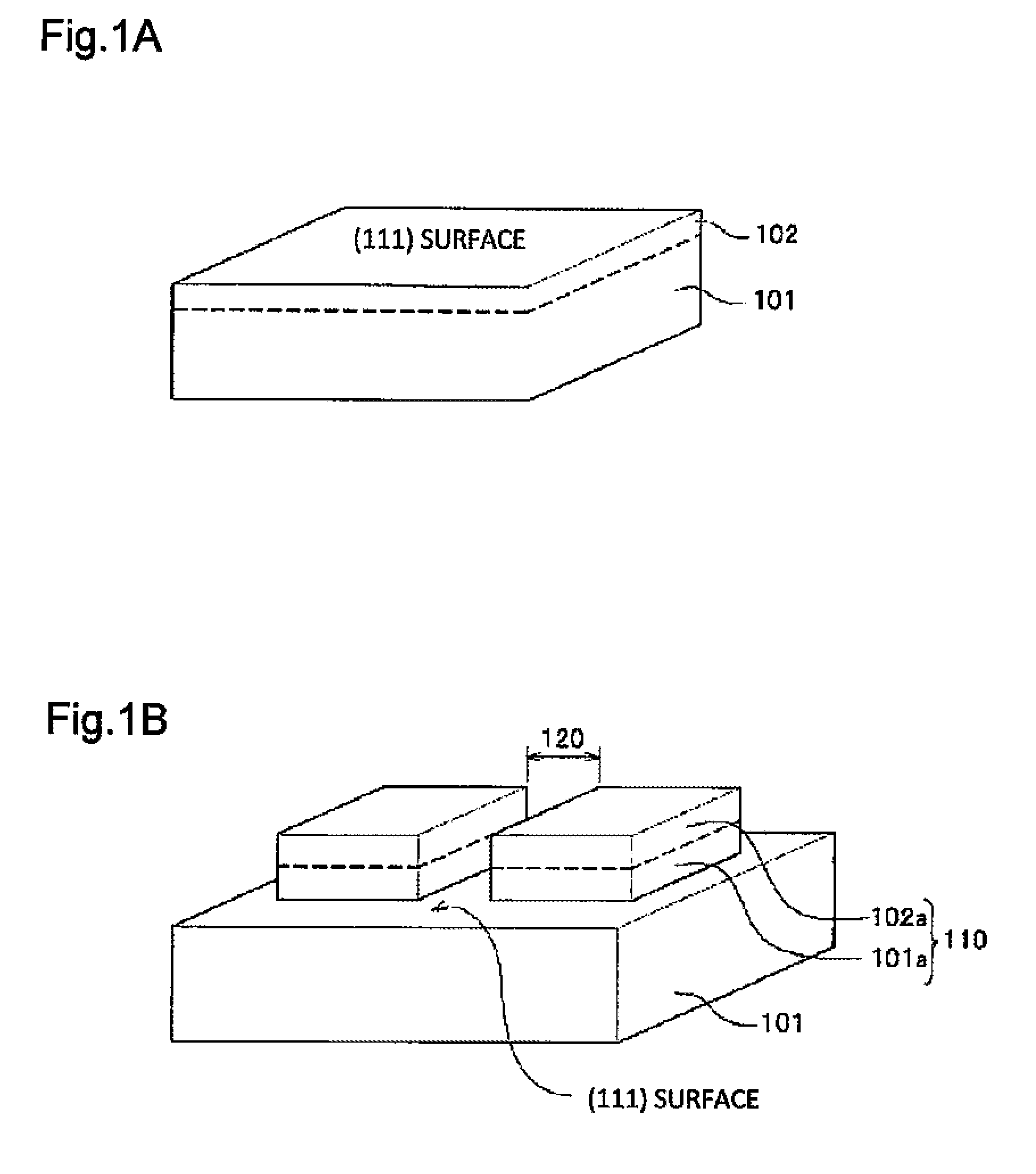
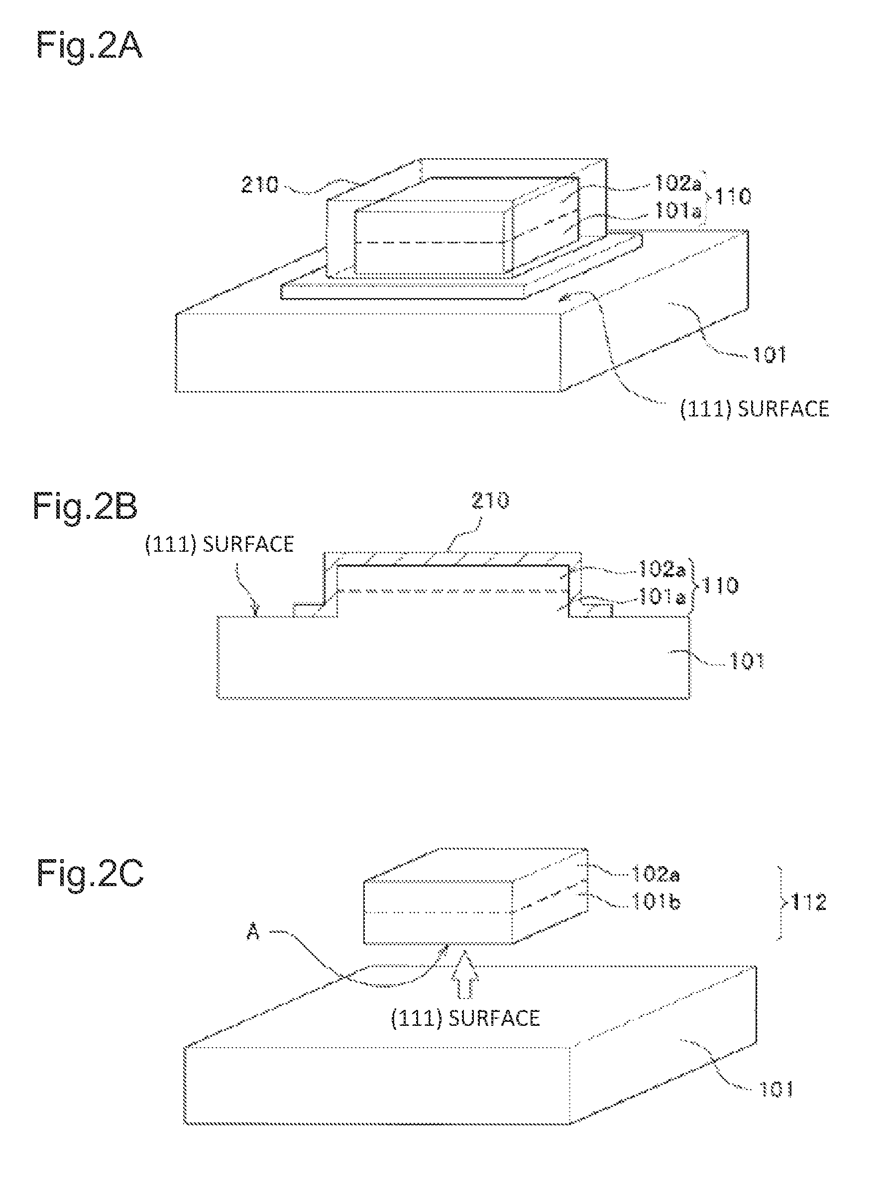
[0029]A first embodiment of the invention is described with reference to FIG. 1 to FIG. 5.

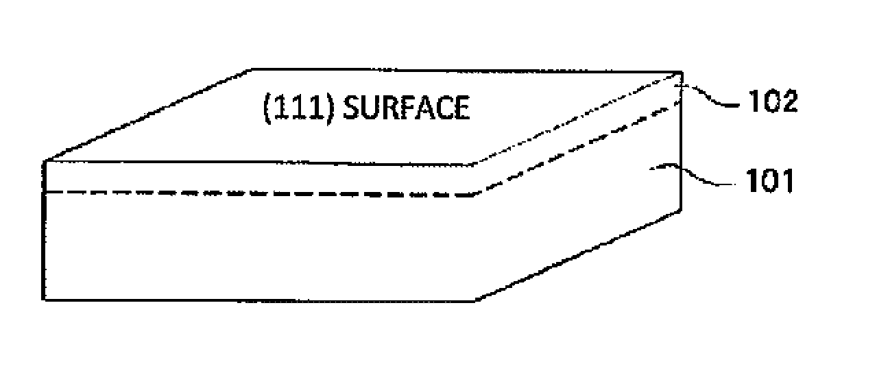
[0030]FIG. 1A is a perspective view showing a configuration of Si (111) substrate 101, which is a first substrate, and circuit / device forming region 102 on the surface of Si (111) substrate 101. FIG. 1B is a perspective view showing a step of forming isolated islands 110 by forming an isolation region 120 in a depth direction from the surface of Si (111) substrate 101 of the first substrate. Each of the isolated islands 110 includes isolated circuit / device forming region 102a and isolated substrate region 101a which are part of Si (111) substrate 101 of the first substrate.

[0031]In FIG. 1A, circuit / device forming region 102 is a region in which an integrated circuit including junctions, capacitors, resistors and the like, and a circuit / device such as a single device, a composite devices or the like is formed in Si (111) substrate 101 of the first substrate. The thickness of circuit / device formi...

second embodiment

[0072]A second embodiment of the invention is described with reference to FIG. 6A and FIG. 6B. The second embodiment provides a semiconductor composite chip in which the single crystal Si (111) thin-film device described in the first embodiment (hereinafter referred to as an Si (111) thin-film integrated device) and one-dimensionally arranged light emitting devices (hereinafter referred to as a single crystal compound semiconductor thin film) are bonded and integrated on a single substrate, the Si (111) thin-film integrated device including the circuit / device forming regions separated from the Si (111) substrate.

[0073]FIG. 6A is a plan view for illustrating semiconductor composite chip 3010 of the embodiment. In semiconductor composite chip 3010 single crystal compound semiconductor thin film 1010 and Si (111) thin-film integrated device 1040 are bonded and integrated on a surface of substrate 1001.

[0074]For example, substrate 1001 is a Si substrate. In addition, substrate 1001 may ...

third embodiment

[0087]In a third embodiment of the invention, with reference to FIG. 7 and FIG. 8, a description is given of a configuration of a one dimensional light emitting device array light source in which multiple semiconductor composite chips are arranged one-dimensionally. Each of the semiconductor composite chips includes single crystal compound semiconductor thin film 1010 and Si (111) thin-film integrated device 1040 which are integrated therein, as described in the second embodiment.

[0088]In FIG. 7, one-dimensional light emitting device array source 4000 includes multiple semiconductor composite chips 3010 which are one dimensionally arranged on wiring substrate 3050, wiring regions 3020, 3030, chip mount region 3040, and connection terminal 3060.

[0089]Wiring substrate 3050 is, for example, a glass epoxy substrate, a metal core wiring substrate including a metal core, a glass substrate, a plastic substrate, a metal substrate, a ceramics substrate or the like.

[0090]Wiring regions 3020, ...


PUM

PropertyMeasurementUnit
thicknessaaaaaaaaaa
areaaaaaaaaaaa
flatnessaaaaaaaaaa

Abstract

A method for manufacturing a semiconductor device, includes: a step of etching a Si (111) substrate along a (111) plane of the Si (111) substrate to separate a Si (111) thin-film device having a separated surface along the (111) plane.

Description

CROSS REFERENCE TO RELATED APPLICATIONS[0001]This application of the invention titled “METHOD OF MANUFACTURING SEMICONDUCTOR DEVICE, SEMICONDUCTOR DEVICE AND SEMICONDUCTOR COMPOSITE DEVICE” is based upon and claims the benefit of priority under 35 USC 119 from prior Japanese Patent Application No. 2009-084099, filed on Mar. 31, 2009, the entire contents of which are incorporated herein by reference.BACKGROUND OF INVENTION[0002]1. Field of the Invention[0003]The invention relates to a method for manufacturing a semiconductor device, a semiconductor device, and a semiconductor composite device, which make it possible, by a low-cost simple process, to obtain a high quality circuit / device forming region having a flat separated surface from a Si substrate.[0004]2. Description of Related Art[0005]Conventionally, a SOI (Silicon on Insulator) substrate has been manufactured by: implanting hydrogen ions in a depth direction from a surface of a first single crystal Si substrate to form a hydr...

Claims


Application Information

Patent Timeline
Patent Type & Authority Patents(United States)
IPC IPC(8): H01L21/30
CPCH01L25/167H01L29/045H01L33/02H01L25/046H01L25/0753H01L33/0079H01L33/60H01L33/62H01L2924/09701H01L2224/48091H01L2924/00014H01L2924/10253H01L2924/00H01L33/0093H10K19/901
Inventor OGIHARA, MITSUHIKOSAGIMORI, TOMOHIKOSUZUKI, TAKAHITOMUTO, MASATAKA
Owner OKI ELECTRIC IND CO LTD
Learn More