Thermal infrared detector and manufacturing method thereof
a technology of infrared detector and manufacturing method, which is applied in the direction of optical radiation measurement, instruments, semiconductor devices, etc., can solve the problems of inability to increase the aperture ratio, the support leg cannot be extended, and the device becomes complex and expensive, and achieves low cost and high sensitiveness.
- Summary
- Abstract
- Description
- Claims
- Application Information
AI Technical Summary
Benefits of technology
Problems solved by technology
Method used
Image
Examples
first embodiment
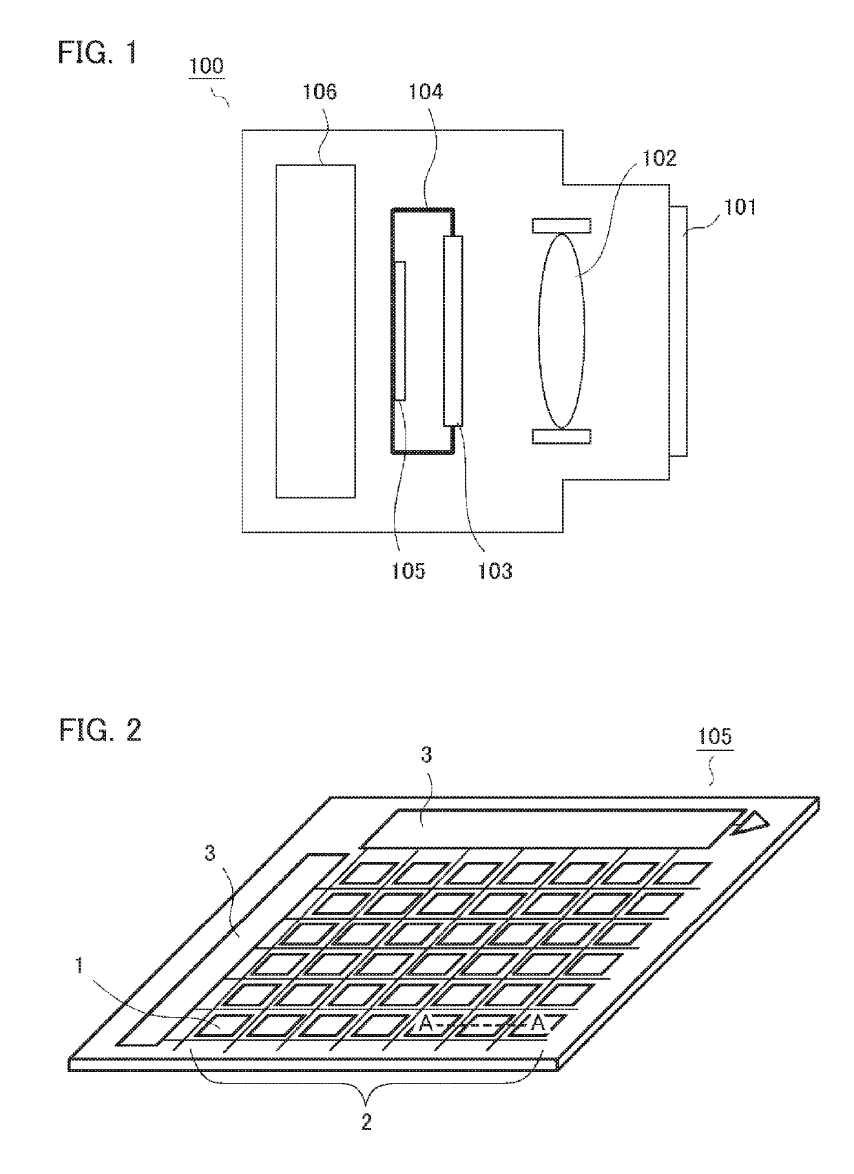
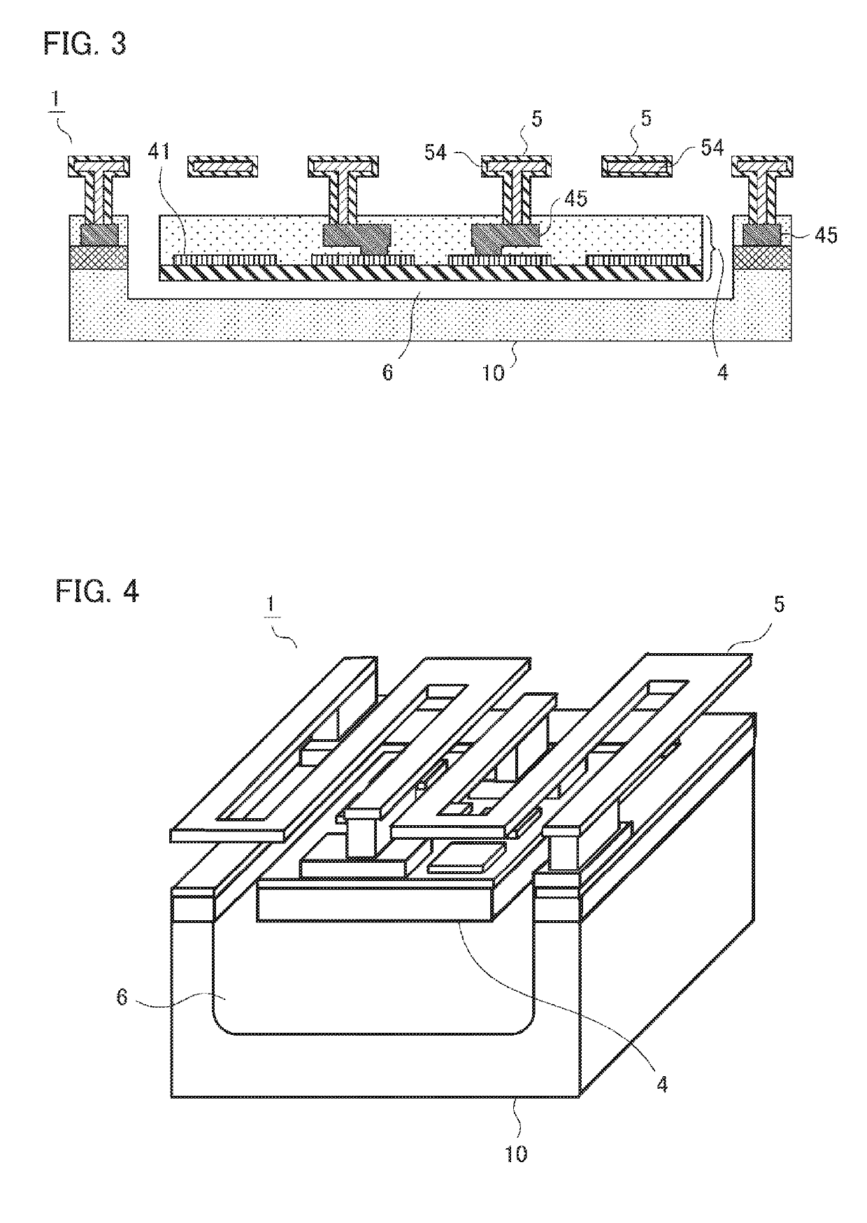
[0029]Hereafter, based on the drawings, a description will be given of a thermal infrared detector, and a manufacturing method thereof, according to a first embodiment of the invention. FIG. 1 is a schematic view of a thermal infrared solid-state imaging device including the thermal infrared detector according to the first embodiment, FIG. 2 is a perspective view showing an infrared image sensor according to the first embodiment, and FIGS. 3 and 4 are a sectional view and a perspective view schematically showing an infrared sensor (a portion indicated by A-A in FIG. 2) according to the first embodiment. The same reference signs are allotted to identical or corresponding portions in the drawings.
[0030]A thermal infrared solid-state imaging device 100 includes a lens protecting window 101 attached to a frame, an optical lens 102 on which infrared rays fall incident, an infrared image sensor 105 housed in a package 104 to which a window material 103 is attached, a signal processing cir...
second embodiment
[0059]An infrared sensor according to a second embodiment of the invention is such that supporting body metal wiring disposed in the supporting body 5 is a layered film including first supporting body metal wiring 54a and second supporting body metal wiring 54b, and one portion of the layered film is oxidized or nitrided. As other configurations are the same as in the first embodiment, only differences from the first embodiment will be described in the following description.
[0060]A method of manufacturing the infrared sensor according to the second embodiment will be described using FIG. 8. FIG. 8 shows a process that follows FIG. 6B, which is described in the first embodiment. The sacrificial layer aperture portion 52 (refer to FIG. 6B) is formed in the predetermined position, the silicon oxide film that is to form the supporting body lower layer film 53 is formed using, for example, PECVD technology so as to cover the sacrificial layer aperture portion 52 on the sacrificial layer ...
third embodiment
[0066]An infrared sensor according to a third embodiment of the invention is such that supporting body metal wiring disposed in the supporting body is a layered film including the first supporting body metal wiring 54a and the second supporting body metal wiring 54b, and one portion of the layered film is oxidized or nitrided, in the same way as in the second embodiment. In the third embodiment, the wiring resistance of the supporting body metal wiring is reduced further than in the second embodiment, because of which the thickness of the first supporting body metal wiring 54a is 70 Å. As other configurations and the manufacturing method are the same as in the first embodiment and the second embodiment, a description will be omitted here.
[0067]FIG. 9 shows an oxygen atom concentration in a depth direction of an oxidized cobalt iron film that configures the supporting body metal wiring of the infrared sensor according to the third embodiment. In FIG. 9, a vertical axis is the oxygen ...
PUM
 Abstract
Description
Claims
Application Information


