
Semiconductor optical device

a technology of semiconductor lasers and optical devices, applied in semiconductor lasers, lasers, laser details, etc., can solve the problems of inability to say that inp and gaas have good thermal conductivity, and limited characteristics, so as to achieve efficient injection of current or application of electric fields, high temperature processing

Active Publication Date: 2022-03-15
NIPPON TELEGRAPH & TELEPHONE CORP
View PDF4 Cites 0 Cited by
  • Summary
  • Abstract
  • Description
  • Claims
  • Application Information

AI Technical Summary

Benefits of technology

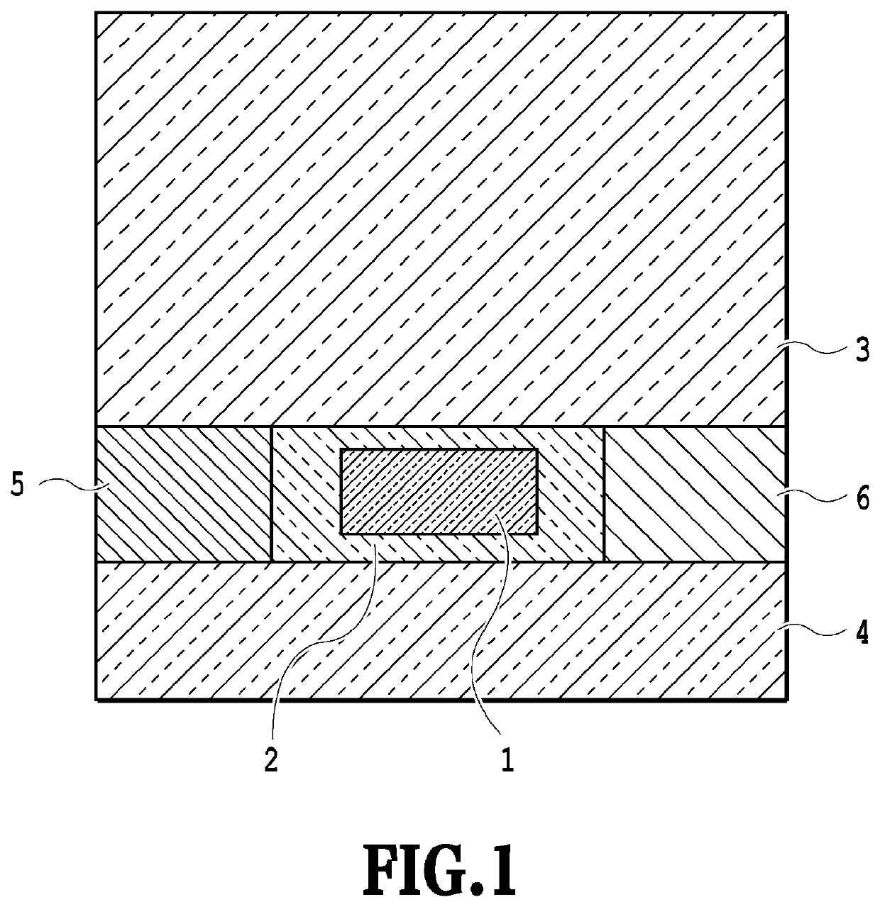
The present invention provides a semiconductor optical device that can efficiently inject current or apply electric field while achieving both heat dissipation and light confinement. Additionally, the device can withstand high temperature processing.

Problems solved by technology

However, materials such as InP and GaAs cannot be said to have a good thermal conductivity, and the characteristics have been limited by a temperature rise due to heat generation during operation of the device (for example, Non-Patent Literature 1).

Method used


Image

  • Semiconductor optical device
  • Semiconductor optical device
  • Semiconductor optical device

Examples


example 1

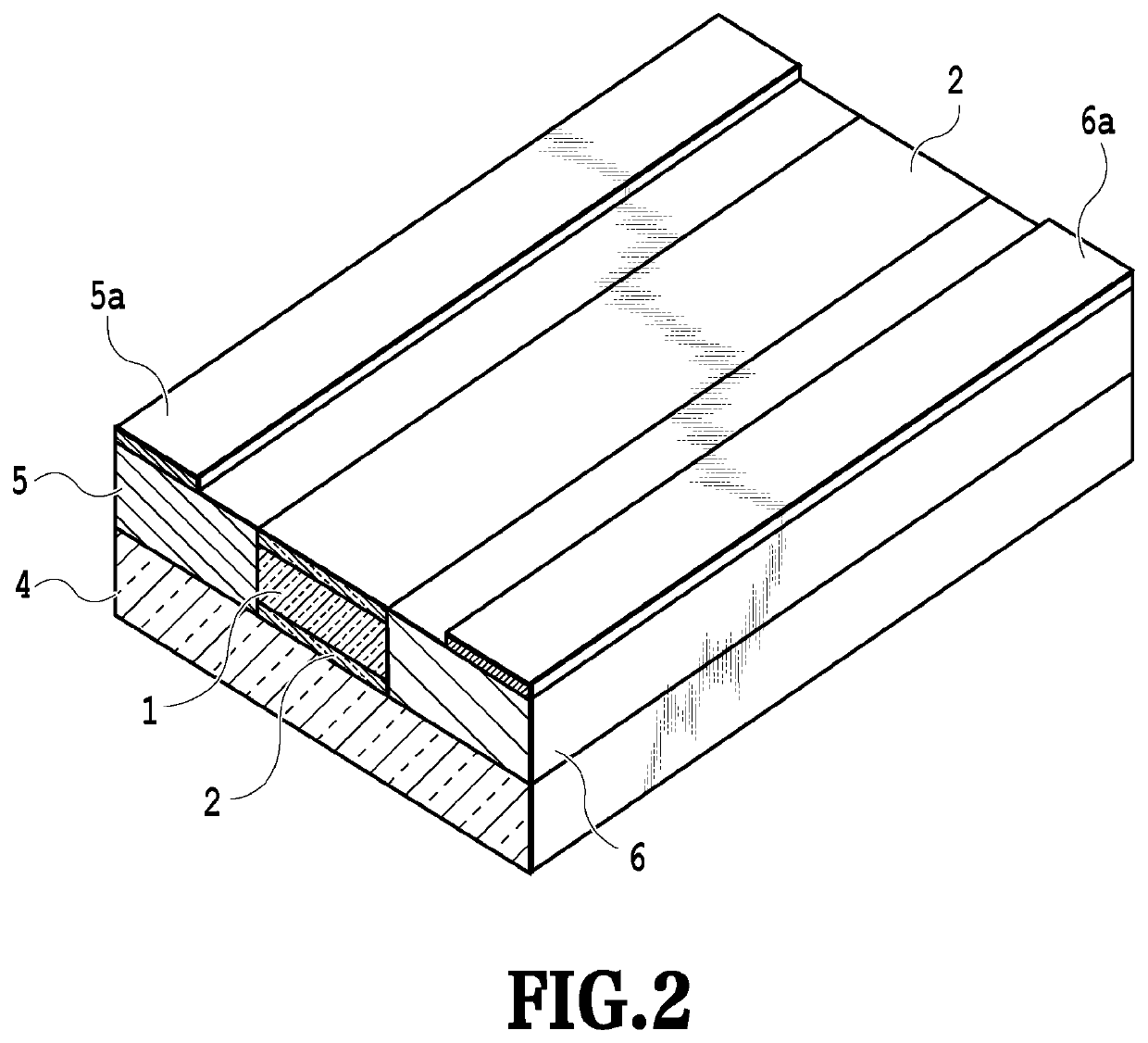
[0066]FIG. 2 is a perspective view showing the structure of the semiconductor optical device according to Example 1 of the present invention. Example 1 of the present invention has a semiconductor laser structure in which current is injected approximately in parallel along the surface of the substrate from the cladding layer 5 to the cladding layer 6 with the active layer 1 sandwiched therebetween as shown in FIG. 2.

[0067]In FIG. 2, the active layer 1 is formed of, for example, InGaAlAs having different compositions as quantum well (MQW) and barrier layer materials, and the core layer (first core layer) is formed by embedding the active layer 1 vertically with the upper and lower optical semiconductor layers 2 (for example, i-InP). The p-type semiconductor layer (p-InP, first cladding layer) 5 and the n-type semiconductor layer (n-InP, second cladding layer) 6 are formed with the core layer sandwiched therebetween, and a contact layer and electrodes 5a and 6a are provided to inject ...

example 2

[0092]The structure of Example 2 of the present invention shown in FIG. 11 differs from that of Example 1 in that the lower cladding (third cladding layer) having a two-layer structure including the SiC substrate 4 and a SiO2 layer 111 is provided by forming the SiO2 layer 111 which is a thin insulating film between the upper layer including the active layer 1, the optical semiconductor layers 2 and the p-type and n-type semiconductor cladding layers 5, 6, and the SiC substrate 4. An insulating film such as the SiO2 layer 111 is considered important in order to suppress void formation at the bonding interface in certain substrate bonding methods.

[0093]This structure of Example 2 shown in FIG. 11 has the two-layer structure in which the lower cladding (third cladding layer) is made of two different materials. One of the two types of materials constituting the third cladding layer is a semiconductor having a large thermal conductivity (SiC being a compound semiconductor), and the othe...

example 3

[0099]FIG. 14 is a cross-sectional structural view of a semiconductor optical device according to Example 3 of the present invention. FIG. 15 is a cross-sectional structural view of a conventionally used semiconductor optical device shown as Comparative Example 2 in comparison with Example 3.

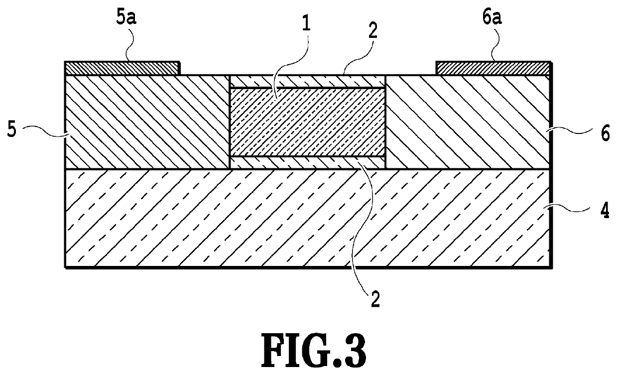
[0100]As shown in FIG. 14, the structure of Example 3 has a first feature such that the upper structure includes a p-type semiconductor layer 5 (first cladding layer) and an n-type semiconductor layer 6 (second cladding layer) which are formed so as to vertically sandwich the multiple quantum well active layer 1 and the optical semiconductor layer 2 to be the first core layer in the thicknesswise direction of the substrate.

[0101]Furthermore, Example 3 has a second feature such that the lower third cladding layer is formed to have a two-layer structure including the SiO2 layer 111 to be the insulating layer and the SiC substrate 4 which serves as the cladding layer and the supporting substrate as...


PUM

PropertyMeasurementUnit
thicknessaaaaaaaaaa
thicknessaaaaaaaaaa
thicknessaaaaaaaaaa

Abstract

A semiconductor optical device that achieves both of heat dissipation and light confinement and permits efficient current injection or application of an electric field is implemented. The semiconductor optical device includes: a core layer including an active region (1) made of a compound semiconductor; two cladding layers (5, 6) injecting current into the core layer; and a third cladding layer (4) made of a material having a larger thermal conductivity, a smaller refractive index, and a larger band gap than a material for any of the core layer and the two cladding layers.

Description

TECHNICAL FIELD[0001]The present invention relates to a semiconductor optical device, and more particularly to a semiconductor optical device having a semiconductor structure which achieves both of high thermal conductivity and high optical confinement by using a cladding of a high thermal conductivity, a high band gap and a low refractive index.BACKGROUND ART[0002]Semiconductor devices are widely used as small-sized, low-power-consuming electronic elements (electronic devices). In particular, semiconductor optical devices including semiconductor lasers that perform light emission, light reception, light modulation and the like are important components that constitute an optical information communication system.[0003]In the optical information communication system, a direct transition type compound semiconductor such as InP (indium phosphorus) or GaAs (gallium arsenide) is mainly used as a material for a semiconductor optical device from the viewpoint of light emission. However, mat...

Claims


Application Information

Patent Timeline
Patent Type & Authority Patents(United States)
IPC IPC(8): H01S5/22H01S5/042
CPCH01S5/222H01S5/042H01S5/0424H01S5/04257H01S5/021H01S5/3214H01S5/0213H01S5/0215H01S5/02461H01S5/34313H01S5/34366H01S5/026
Inventor NAKAO, RYOKAKITSUKA, TAKAAKIMATSUO, SHINJI
Owner NIPPON TELEGRAPH & TELEPHONE CORP
Learn More