Techniques of optical proximity correction using GPU

a technology of optical proximity correction and gpu, applied in the field of electronic design automation, can solve the problems of s, optical proximity correction, and modification of mask shapes for fixed source shapes, and may be very computationally intensive, and may require an even larger number of computational resources

Active Publication Date: 2013-07-16
D2S
View PDF4 Cites 39 Cited by
  • Summary
  • Abstract
  • Description
  • Claims
  • Application Information

AI Technical Summary

Benefits of technology

[0007]A technique of the invention uses optical proximity correction on hardware or software platforms with graphics processing units. Optical proximity correction techniques performed on one or more graphics processors improve the masks used for the printing of microelectronic circuit designs.

Problems solved by technology

Unfortunately, just the modification of the mask shapes for a fixed source shape, S, known as optical proximity correction, may be very computationally intensive.
Furthermore, inverse lithography technology (ILT), which may provide better results, may be even more computationally intensive, requiring an even larger number of computational resources than traditional OPC.
However, this approach can lead to poor printing quality because the user cannot always select the layout portions necessary for a globally optimal result.
In addition, there may not be a single source shape that would optimize all the shapes in the layout.
The computational complexity of a source shape initialization algorithm can be very high if special care is not taken.
In another implementation, these sample points are not uniform.
The calculations are computational complex.
Although this produces a solution, this infeasible solution is expected to be far from the feasible binary solution which then produces a sub-optimal result.
Although this produces a solution, this solution is expected to be far from a feasible binary solution which then produces a suboptimal result.
This algorithm is computational complex.

Method used


Image

  • Techniques of optical proximity correction using GPU
  • Techniques of optical proximity correction using GPU
  • Techniques of optical proximity correction using GPU

Examples


case 1

[0069]By dividing the index space, n1 or n2, into equal intervals, the hnk1 with a lower degree polynomial can be approximated. The interval in which the given n1 or n2 values lie can be determined by dividing the index by the interval length and by using a switching operation (described below). If a 3rd degree polynomial approximation is used, the calculation cost can be reduced to 4 multiplications and a switching operation.[0070]IntervalLength=totalIntervalLength / 10; / / as an example[0071]interval=n1 / IntervalLength;[0072]switch (interval)[0073][0074]hnk1=((c3*x+c2)*x+c1)*x+c0;[0075]break;[0076]case 2:[0077]hnk1=((c7*x+c6)*x+c5)*x+c4;[0078]break;[0079]. . .[0080]}

[0081]In other words, the total cost can be reduced. In the above example, the total cost can be reduced to 8×(4+1)=40 computations, which is about 5× faster than the ones employing memory lookup operations.

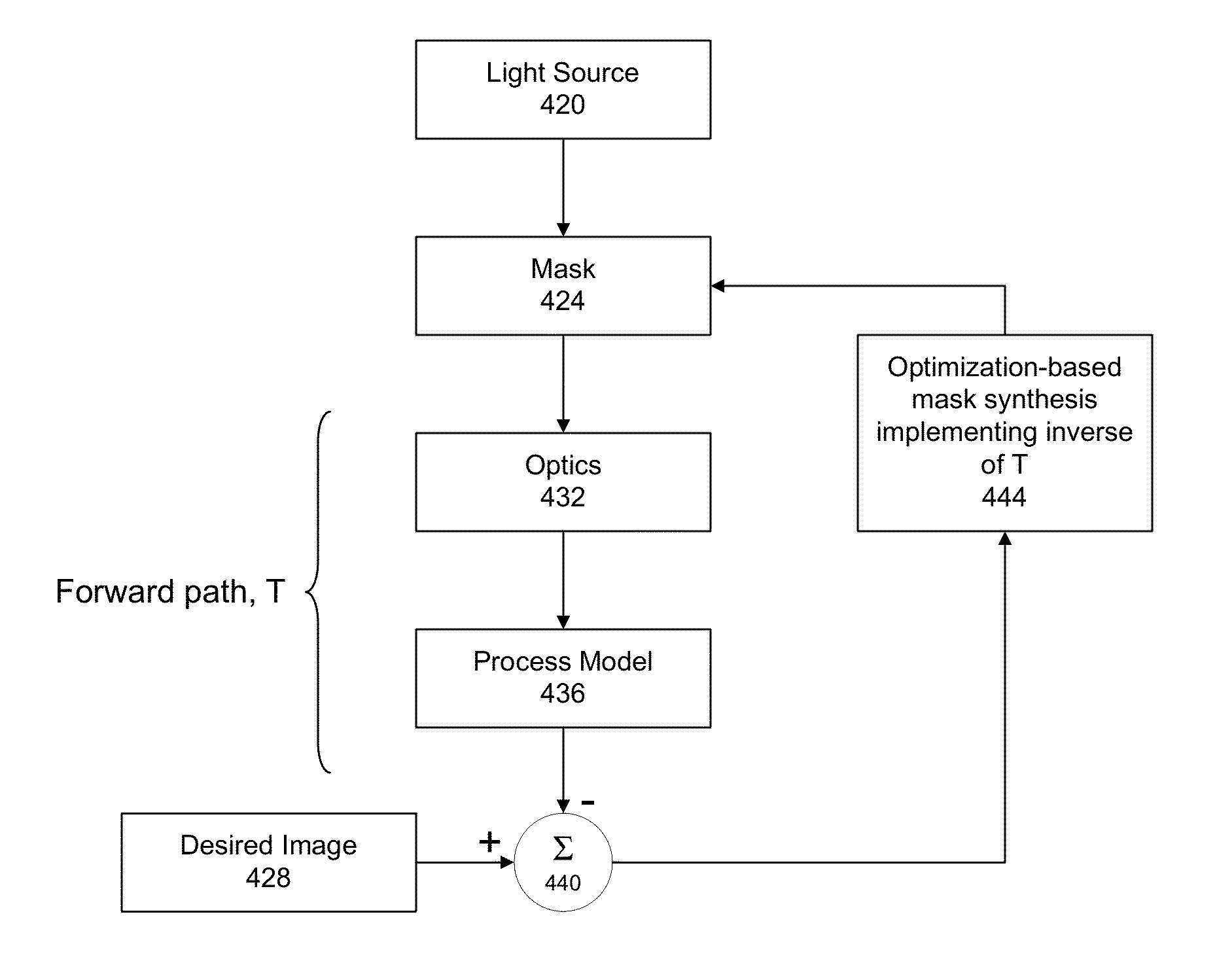
[0082]Section 3 Optical Proximity Correction on Hardware or Software Platforms with Graphical Processing Units

[0083]T...


PUM


Abstract

Computationally intensive electronic design automation operations are accelerated with algorithms utilizing one or more graphics processing units. The optical proximity correction (OPC) process calculates, improves, and optimizes one or more features on an exposure mask (used in semiconductor or other processing) so that a resulting structure realized on an integrated circuit or chip meets desired design and performance requirements. When a chip has billions of transistors or more, each with many fine structures, the computational requirements for OPC can be very large. This processing can be accelerated using one or more graphics processing units.

Description

CROSS-REFERENCE TO RELATED APPLICATIONS[0001]This application claims priority to U.S. provisional patent application 61 / 362,565, filed Jul. 8, 2010, which is incorporated by reference along with all other references cited in this patent application.BACKGROUND OF THE INVENTION[0002]The present invention relates to the field of electronic design automation and, in particular, to improved techniques for computationally efficient and accurate optical proximity correction.[0003]Optical proximity correction or OPC is a photolithography enhancement technique commonly used to compensate for image errors due to diffraction or process effects. The need for OPC is seen mainly in the making of semiconductor devices and is due to the limitations of light to maintain the edge placement integrity of the original design, after processing, into the etched image on the silicon wafer. These projected images appear with irregularities such as line widths that are narrower or wider than designed, these ...

Claims


Application Information

Patent Timeline
Patent Type & Authority Patents(United States)
IPC IPC(8): G06F17/50
CPCG06F17/5068G06F17/50G06F2217/12G06F2119/18G06F30/39Y02P90/02G06F30/00G03F7/70441
Inventor TORUNOGLU, ILHAMI H.KARAKAS, AHMETELSEN, ERICH E.
Owner D2S
Why Eureka
Try Eureka