SRAM cell with common bit line and source line standby voltage

a technology of source line and memory cell, which is applied in the direction of static storage, information storage, digital storage, etc., can solve the problems of failure to meet the low standby power objective, failure to write logic 1 value into the fig. 3 bit cell, and large transistors consuming additional integrated circuit silicon area and power, etc., to achieve maximum read-noise margin, reduce standby leakage power, and save space

Inactive Publication Date: 2013-08-06
HOBSON RICHARD FREDERIC +1
View PDF13 Cites 72 Cited by
  • Summary
  • Abstract
  • Description
  • Claims
  • Application Information

AI Technical Summary

Benefits of technology

[0013]The invention permits maximal area savings in a 5 T SRAM bit cell while using high threshold transistors and a raised source virtual ground voltage for reduction of standby leakage power. During memory block standby, bit cell virtual ground lines and BIT lines are all connected to a common standby voltage, Vsb, which is chosen to maximize read-noise-margin while also safely maintaining bit cell data. During a memory block read, bit cell sub-column virtual ground lines are driven to Gnd at the same time, or somewhat before the word line is driven to a value 10% to 20% above logic 1 voltage, Vdd. BIT line voltages, which start at Vsb, are either pulled substantially lower, or slightly higher by activated bit cells, and sensed by sense amplifiers that connect to BIT l

Problems solved by technology

Consequently, the operation of writing a logic 1 value into the FIG. 3 bit cell may fail or require an unacceptably long period of time.
One way to compensate for this is to preferentially adjust the sizes (and possibly thresholds) of the transistors in inverters 1, 2, as well as transistor N3, so that a “weak” logic 1 value driven onto inverter 1's node Q, more easily cross-couples through node Q and inverter 2 to complete the writing event at node Q. While this technique can be made to work, as taught by Carlson et al (European Solid-State Circuits Conference, ESSCIRC, 2004, pp 215-218), the drawback is that larger transistors consume additional integrated circuit silicon area and power.
It also fails to meet the low standby power objective.
A disadvantage of the control circuitry in FIG. 5 is that the number of transistors used to control Vd1, Vd2 and Vg1, Vg2 is significant, thereby reducing th

Method used


Image

  • SRAM cell with common bit line and source line standby voltage
  • SRAM cell with common bit line and source line standby voltage
  • SRAM cell with common bit line and source line standby voltage

Examples


Embodiment Construction

[0026]Throughout the following description, specific details are set forth in order to provide a more thorough understanding of the invention. However, the invention may be practiced without these particulars. In other instances, well known elements have not been shown or described in detail to avoid unnecessarily obscuring the invention. Accordingly, the specification and drawings are to be regarded in an illustrative, rather than a restrictive, sense.

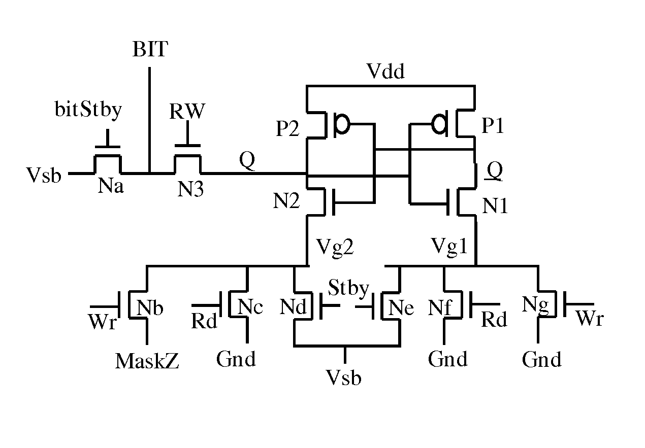
[0027]Large memories are hierarchically constructed from smaller memory building blocks (MBB). Within the lowest level of such a block, BIT lines may run through a column that is further divided into sub-columns. For example, a column containing 128 bit cells may be sub-divided into 2 64-bit or 4 32-bit sub-columns. During primary decoding, only 1 bit cell of a column is accessed at a time. Multiple columns are arranged in an array to form rows and columns. A row of bit cells may contain 1 or more words of bits, where a word is the sm...


PUM


Abstract

A high threshold five transistor SRAM bit cell with cross-coupled inverters has a single BIT line, a common logic 1 supply voltage, and two logic 0 virtual ground source voltages. The BIT line is coupled to the bit cell by a pass transistor. When BIT line and virtual ground lines are not otherwise being used, they are connected to a common standby voltage that substantially lowers bit cell standby leakage. Writing is performed by driving a data signal through the pass transistor and is facilitated by creating a voltage differential on the virtual ground lines. Reading is also performed through the pass transistor wherein the BIT line is initially at the standby voltage, and is then driven lower or higher depending upon the data value stored in the bit cell.

Description

FIELD OF THE INVENTION[0001]This invention relates to a five transistor static random access memory cell, particularly when the standby power of the memory cell and its associated bit line are to be reduced.BACKGROUND OF THE INVENTION[0002]FIGS. 1 and 2 schematically depict a typical prior art single binary digit (i.e. 1-bit) six-transistor (6 T) SRAM bit cell incorporating cross-coupled inverters 1, 2. Inverter 1 is formed by PMOS “pull-up” transistor P1 and NMOS “pull-down” transistor N1, as shown in FIG. 2. PMOS transistor 1's source is connected to a logic 1 voltage reference (Vd1==Vdd), PMOS transistor 1's drain is connected in series with NMOS transistor 1's drain, NMOS transistor 1's source is connected to a logic 0 voltage reference (Vg1==system ground, Gnd), and PMOS transistor 1's gate is connected to NMOS transistor 1's gate. Inverter 2 is formed by PMOS pull-up transistor P2 and NMOS pull-down transistor N2. PMOS transistor P2's source is connected to Vd2 (==Vdd), PMOS t...

Claims


Application Information

Patent Timeline
IPC IPC(8): G11C11/00
CPCG11C11/412
Inventor HOBSON, RICHARD FREDERICJAROLLAHI, HOOMAN
Owner HOBSON RICHARD FREDERIC
Why Eureka
Try Eureka