
Class of soluble, photooxidatively resistant acene derivatives

a technology of acene derivatives and acene, which is applied in the field of soluble, photooxidatively resistant acene derivatives, can solve the problems of poor solubility, propensity to photo-oxidize, and hinder the application of thin-film electronic devices, and achieve the effect of improving electronic characteristics considerably

Inactive Publication Date: 2013-08-20
UNIVERSITY OF NEW HAMPSHIRE
View PDF18 Cites 1 Cited by
  • Summary
  • Abstract
  • Description
  • Claims
  • Application Information

AI Technical Summary

Benefits of technology

The patent text discusses the importance of π-π-stacking interactions in organic semiconductor thin film compounds and materials. These interactions can lead to a stack structure, which results in a stronger conjugated plane and improved electronic characteristics compared to a herringbone structure. The technical effect is to improve the performance of organic semiconductor thin film compounds and materials by optimizing π-π-stacking interactions.

Problems solved by technology

However, its application in thin-film electronic devices is hindered by its poor solubility and its propensity to photo-oxidize (Ono, K., et al., Tetrahedron, 2007, 61:9699-9704; Palayangoda, S. S., et al., J. Org. Chem., 2007, 72:6584-6587; Etienne, A. and C. Beauvios, Compt. Rend., 1954, 239:64-66; Benor, A., et al., Org.
Pentacene oxidation leads to diminished electronic device performance.

Method used


Image

  • Class of soluble, photooxidatively resistant acene derivatives
  • Class of soluble, photooxidatively resistant acene derivatives
  • Class of soluble, photooxidatively resistant acene derivatives

Examples


Embodiment Construction

Compounds of the Present Invention

[0017]The compounds of the present invention relate to novel and non-obvious acene derivatives. Acenes or large acenes or oligoacenes or polyacenes are a class of organic compounds and polycyclic aromatic hydrocarbons made up of linearly fused benzene rings. Pentacene contains five linearly fused benzene rings. Although the structure of pentacene resembles that of other aromatic compounds like anthracene, its aromatic properties are poorly defined by those of skill in the art and; as such, pentacene and its derivatives are the subject of much research.

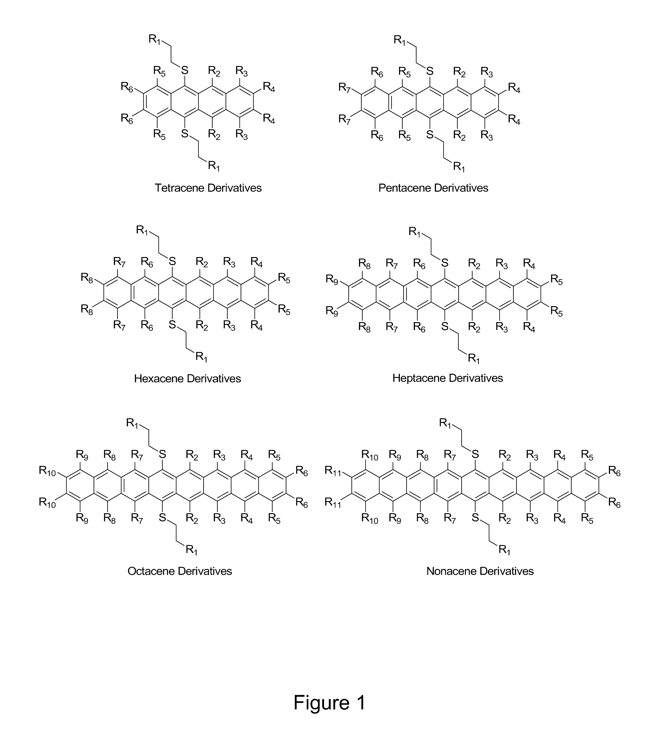
[0018]The compounds of the present invention are acene derivatives bearing functional groups. FIG. 1 shows a schematic of the generic compounds of the present invention where R1 is selected from, without limitation, carbonyl moieties, alkene moieties, alkyne moieties, diene moieties and aromatic moieties of all types. R2 through R11 represent any group chosen from the following list: hydrogen, alkyl (e...


PUM

PropertyMeasurementUnit
hole mobilityaaaaaaaaaa
thicknessaaaaaaaaaa
thicknessaaaaaaaaaa

Abstract

The present invention is directed towards a new class of semi-conducting acene derivatives. These compounds are all soluble species and they all possess superior resistance to photooxidation as compared to their counterparts that lack the substitution patterns disclosed herein.

Description

[0001]The authors acknowledge the National Science Foundation (Nanoscale Science & Engineering Center for High-rate Nanomanufacturing, NSF-0425826) for financial support of this work. The Federal Government has a nonexclusive, nontransferable, irrevocable license in this invention on behalf of the United States. [37 CFR 401.14(b)].BACKGROUND OF INVENTION[0002]Traditionally, inorganic materials have dominated the electronic device industry. For example, silicon arsenide and gallium arsenide have been used as semiconductor materials, silicon dioxide has been used as an insulator material, and metals such as aluminum and copper have been used as electrode materials. In recent years, however, there has been an increasing research effort aimed at using organic materials rather than the traditional inorganic materials in electronic devices. Among other benefits, the use of organic materials may enable lower cost manufacturing of electronic devices, may enable large area applications, and ...

Claims


Application Information

Patent Timeline
Patent Type & Authority Patents(United States)
IPC IPC(8): C07C323/31
CPCC07C321/28C07C323/09
Inventor MILLER, GLEN P.KAUR, IRVINDER
Owner UNIVERSITY OF NEW HAMPSHIRE
Learn More