Semiconductor device manufacturing method and manufacturing apparatus

a technology of semiconductor devices and manufacturing methods, applied in the direction of transistors, basic electric elements, electrical equipment, etc., can solve the problems of inability to bring wafers, poor appearance due to residues, and more likely to remain residues, so as to achieve sufficient ultraviolet irradiation and reduce irradiation time

Active Publication Date: 2013-08-27
FUJI ELECTRIC CO LTD
View PDF11 Cites 0 Cited by
  • Summary
  • Abstract
  • Description
  • Claims
  • Application Information

AI Technical Summary

Benefits of technology

[0035]An object of the invention is to provide a semiconductor device manufacturing method and manufacturing apparatus with which it is possible, when a wafer has a warp, to effectively peel off an ultraviolet peelable tape with ultraviolet irradiation of a short duration.
[0046]According to the invention, even when a wafer has a warp, by irradiating the wafer with ultraviolet light after correcting the warp of the wafer in advance, it is possible to approximately uniformly irradiate an ultraviolet peelable tape attached to the wafer with the ultraviolet light. Also, it is possible to obtain a sufficient ultraviolet irradiation amount appropriate for peeling off the ultraviolet peelable tape, and achieve a reduction in irradiation time.

Problems solved by technology

In particular, the smaller the thickness of the wafer 1, the smaller the heat capacity of the wafer 1, meaning that the rise in temperature increases, a residue is more likely to remain, and a poor appearance occurs due to the residue.
Meanwhile, when a fluorescent tube type black light or ultraviolet light emitting diode with little heat generation is used as the ultraviolet light source 13, it is possible to suppress the rise in temperature of the wafer 1, but as there is no little heat generation from the lamp itself, it is not possible to bring the wafer 1 into contact with, or close to, the lamp.
For this reason, there is a problem in that an irradiation time of several minutes to a dozen minutes or so is necessary in order to obtain an ultraviolet irradiation amount of 1000 mJ / cm2 or more necessary for peeling, and a throughput (a manufacturing man-hour) decreases.
For this reason, when the wafer 1 has a warp, the throughput decreases, and a manufacturing cost increases.
As another method of correcting the warp of the wafer, a method is conceivable whereby the wafer is adsorbed by a porous chuck or an electrostatic chuck but, as it is also difficult in this case to adsorb the wafer without correcting the warp of the wafer at all, an auxiliary mechanism for correcting the warp of the wafer is necessary, meaning that there has been a problem in that a wafer support mechanism is complicated, increasing the cost.

Method used


Image

  • Semiconductor device manufacturing method and manufacturing apparatus
  • Semiconductor device manufacturing method and manufacturing apparatus
  • Semiconductor device manufacturing method and manufacturing apparatus

Examples


working example 1

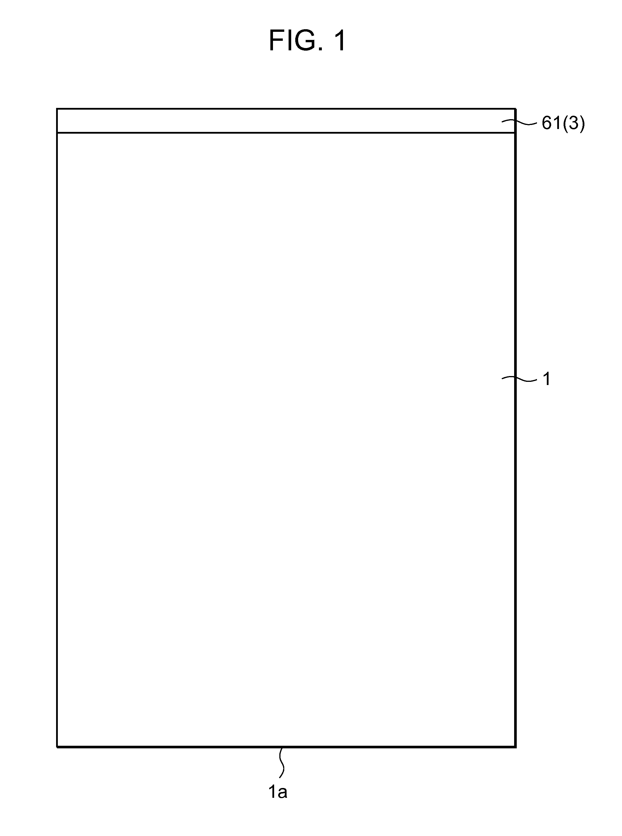
[0072]FIGS. 1 to 11 are main portion manufacturing step sectional views showing in the order of steps a semiconductor device manufacturing method of a first working example of the invention. Herein, a planar field stop (FS) IGBT formed on a thin silicon wafer 1 is taken up as a semiconductor device.

[0073]Firstly, a surface structure 61 configured of a p-well layer 52, an n-emitter layer 53, a gate electrode 55, an emitter electrode 56, and an interlayer insulating film 57, shown in FIG. 24, is formed on a surface layer of the n-type wafer 1 (FIG. 1). None of the portions configuring the surface structure 61 is shown in FIG. 1. Also, at this stage, the emitter electrode 56 of FIG. 24 is formed from an aluminum-silicon film 3.

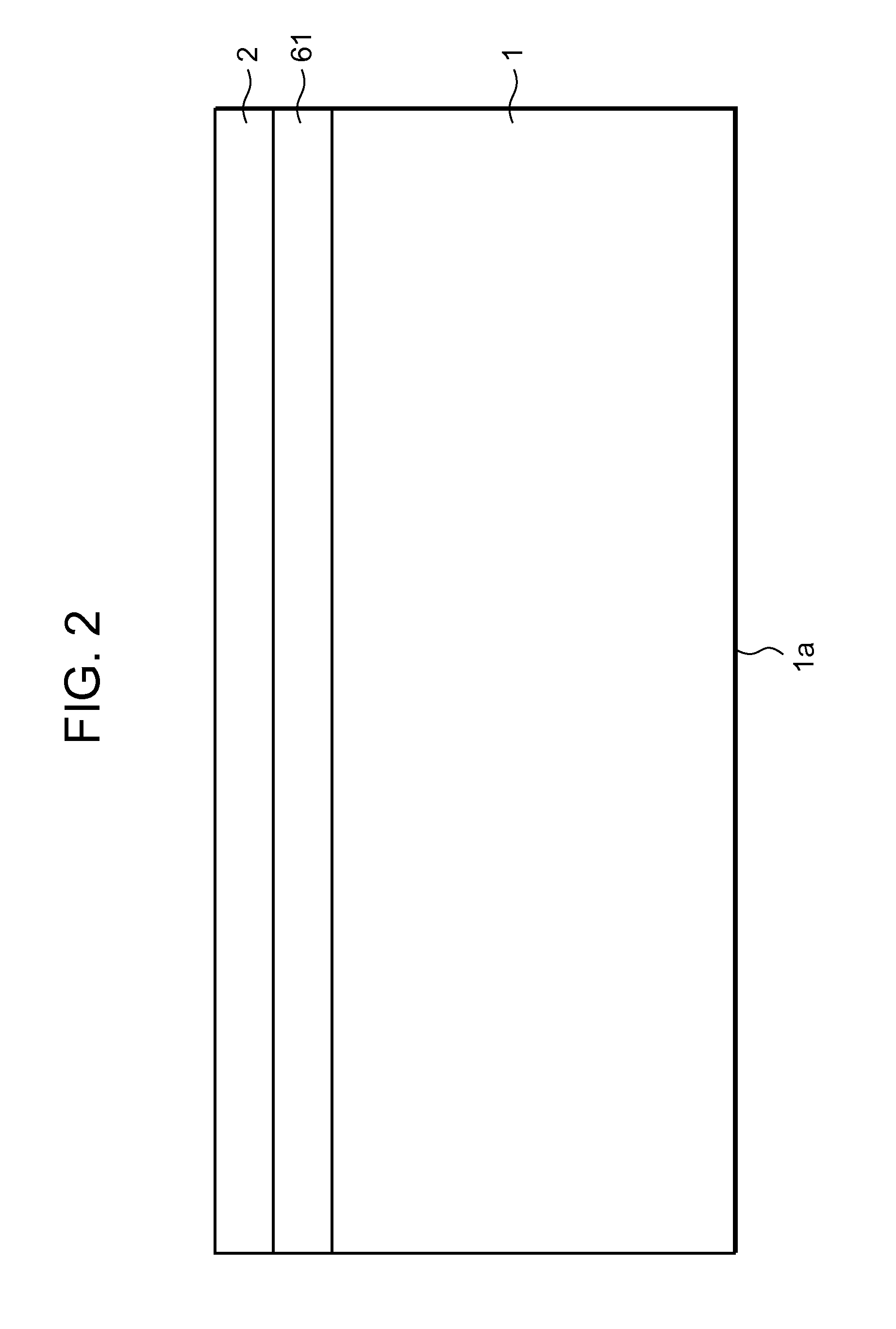
[0074]Next, the surface structure 61 is attached to a grinding protection tape 2 (a backgrinding tape), and a wafer rear surface 1a is ground, reducing the thickness of the wafer 1 (FIG. 2). The thickness of the wafer 1 is in the order of 80 μm for a product with...

working example 2

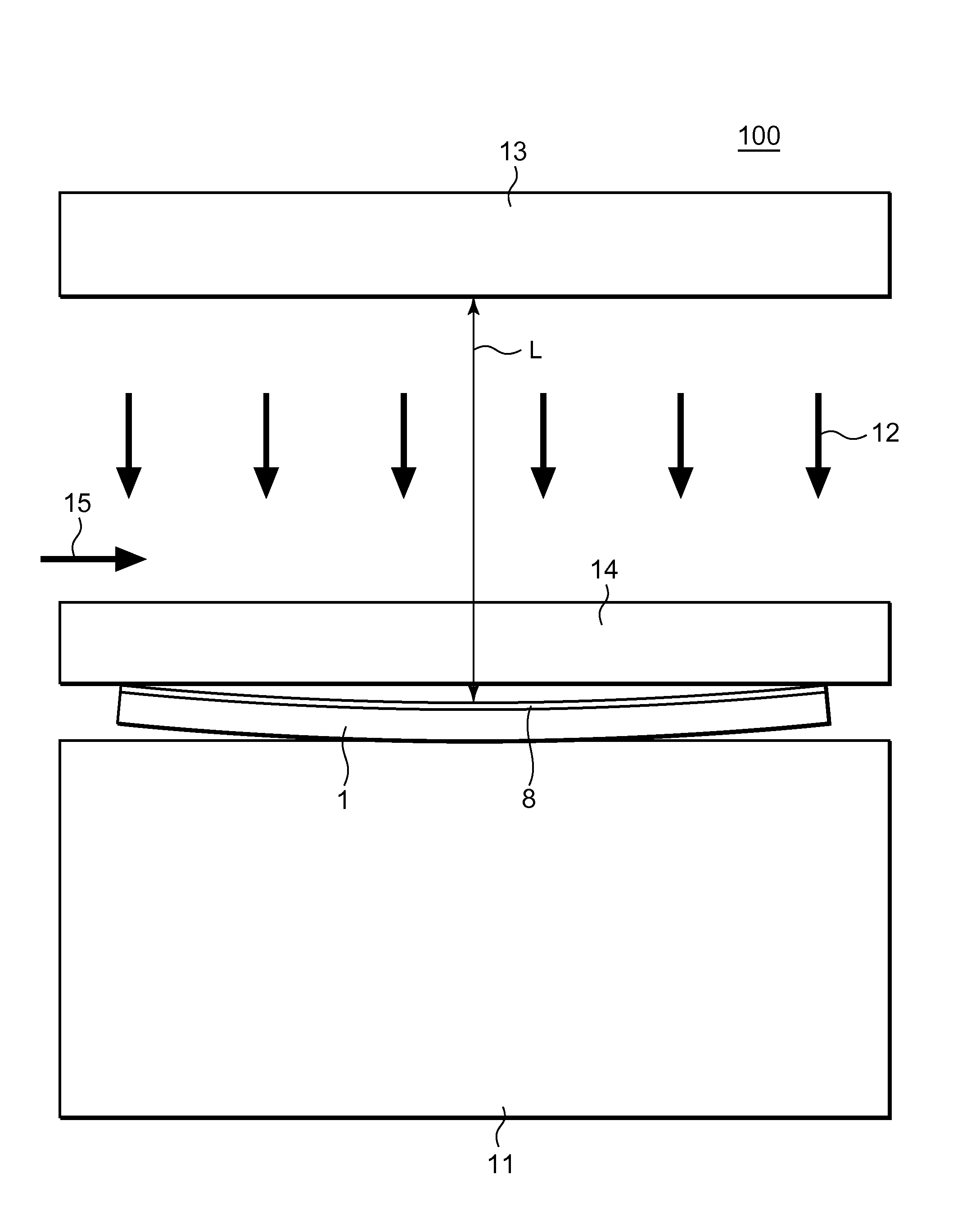
[0096]FIG. 13 is a main portion configuration diagram of a semiconductor device manufacturing apparatus of a second working example of the invention. The manufacturing apparatus is an ultraviolet irradiation apparatus 100 suitable for peeling off an ultraviolet peelable tape 8 attached to a wafer 1. The ultraviolet irradiation apparatus 100 shown here is an example of a top irradiation type.

[0097]The ultraviolet irradiation apparatus 100 is configured of a support 11 which is movable up and down, and on which the wafer 1 is placed, an ultraviolet transmitting plate 14 disposed on the support 11, and an ultraviolet light source 13 which, being disposed on the ultraviolet transmitting plate 14, irradiates the ultraviolet peelable tape 8 attached to the wafer 1 with ultraviolet light 12.

[0098]Strength (a thickness) of such an extent that it is possible to correct a warp of the wafer 1 may be provided in the support 11 so that the support 11 will not bend even by the warped wafer 1 bein...


PUM

PropertyMeasurementUnit
thicknessaaaaaaaaaa
thicknessaaaaaaaaaa
breakdown voltageaaaaaaaaaa

Abstract

A semiconductor device manufacturing method and manufacturing apparatus with which it is possible, when a wafer has a warp, to effectively peel off an ultraviolet peelable tape with ultraviolet irradiation of a short duration. Even when a wafer has a warp, by correcting the warp of the wafer with an ultraviolet transmitting plate, and uniformly irradiating an ultraviolet peelable tape attached to the wafer with ultraviolet light, it is possible to reduce a distance between an ultraviolet light source and the ultraviolet peelable tape. Also, by blocking heat from the ultraviolet light source with the ultraviolet transmitting plate, it is possible to suppress a rise in temperature of the wafer. As a result of this, it is possible to effectively peel the ultraviolet peelable tape from the wafer with ultraviolet irradiation of a short duration without any adhesive residue remaining.

Description

CROSS REFERENCE TO RELATED APPLICATION[0001]The entire disclosure of the inventor's corresponding Japanese patent application, Ser. No. JP PA 2010-236205, filed Oct. 21, 2010, is hereby incorporated by reference.BACKGROUND OF THE INVENTION[0002]1. Technical Field[0003]The present invention relates to a manufacturing method of a semiconductor device formed from a thin semiconductor wafer, such as a field stop (FS) insulated gate bipolar transistor (IGBT), and to a manufacturing apparatus thereof.[0004]2. Related Art[0005]Among manufacturing steps of a semiconductor device formed from a thin silicon wafer (hereafter simply called a wafer), such as an FS IGBT, after a surface structure of a semiconductor element is made on the upper surface of the wafer, there is a step of grinding the rear surface of the wafer, thus carrying out a reduction in film thickness (hereafter simply called “a reduction in thickness”). In the wafer rear surface grinding step, after a grinding protection tape,...

Claims


Application Information

Patent Timeline
Patent Type & Authority Patents(United States)
IPC IPC(8): H01L21/301H01L21/46H01L21/78
CPCH01L29/66333H01L21/67115Y10T29/41
Inventor URANO, YUICHI
Owner FUJI ELECTRIC CO LTD
Why Eureka
Try Eureka