Two-beam laser annealing with improved temperature performance

a laser annealing and temperature performance technology, applied in semiconductor/solid-state device testing/measurement, semiconductor/solid-state device details, manufacturing tools, etc., can solve the problem of temperature overshoot, edge damage near features, and potential large within-chip temperature non-uniformities, etc. problem, to achieve the effect of improving the temperature uniformity of the wafer surfa

Active Publication Date: 2013-10-01
VEECO INSTR
View PDF54 Cites 23 Cited by
  • Summary
  • Abstract
  • Description
  • Claims
  • Application Information

AI Technical Summary

Benefits of technology

[0007]Aspects of the disclosure include systems and methods for performing laser annealing using two laser beams having different wavelengths, while other aspects of the disclosure use two laser beams having the same wavelength but a different configuration, i.e., at least one of a different polarization, a different angle of incidence and a different plane of incidence. The systems and methods improve the temperature uniformity of the wafer surface during the annealing process. For wafers whose annealing temperature is limited by slip generation, the two-beam annealing systems and methods disclosed herein can be used to increase the maximum annealing temperature that can be applied without causing slip.
[0008]Measurements performed on semiconductor wafers indicate that the wafer surface reflectivity can vary significantly as a function of wafer surface position as well as of the laser wavelength, polarization, angle of incidence and the incident plane orientation with respect to the features formed on the wafer surface. The two-wavelength annealing approach described herein can reduce and in some cases substantially compensate for reflectivity variations and thereby improve the anneal temperature uniformity even within individual IC chips.
[0009]The use of the systems and methods disclosed herein to improve within-chip temperature uniformity (as compared to conventional single-beam annealing approaches) is particularly useful when annealing wafers having devices formed with materials that cause high surface reflectivity at infrared wavelengths. In this case, the ratio of the intensities of the two laser beams can be optimized or can be varied as a function of wafer surface position to achieve a minimum optical absorption contrast, which in turn leads to improved anneal temperature uniformity.
[0011]A second aspect of the disclosure is a method of combining two laser beams to improve the annealing temperature uniformity as described above, and further includes performing the annealing based on reflectivity maps at the preheat and anneal wavelengths and for the portion of the wafer surface to be annealed. Thus, the method includes measuring the reflectivity of at least a portion of the wafer surface for the respective preheat and anneal wavelengths λ1 and λ2 to obtain first and second reflectivity maps. Then, using the first and second reflectivity maps, the method also includes annealing the wafer surface using first and second laser beam intensities I1 and I2 that reduce the temperature variation in the wafer surface as compared to using a single laser beam for annealing. In an example, at least one of first laser beam intensity I1 and second laser beam intensity I2 is varied as a function of the wafer surface position in a manner that reduces or minimizes variations in the wafer surface temperature as compared to annealing the wafer surface with a single anneal laser beam.

Problems solved by technology

A key challenge to implementing this type of annealing on patterned wafers is the potential large within-chip temperature non-uniformities that can arise from spatial variations in the optical and thermal properties of the wafer surface caused by the features of the IC chip.
However, for certain IC chip features and for layouts involving large features, temperature overshoots have been observed due to optical diffraction at the boundary between two adjacent regions that have different optical properties.
This temperature overshoot can lead to edge damage near features formed in wafer 10.

Method used


Image

  • Two-beam laser annealing with improved temperature performance
  • Two-beam laser annealing with improved temperature performance
  • Two-beam laser annealing with improved temperature performance

Examples


Embodiment Construction

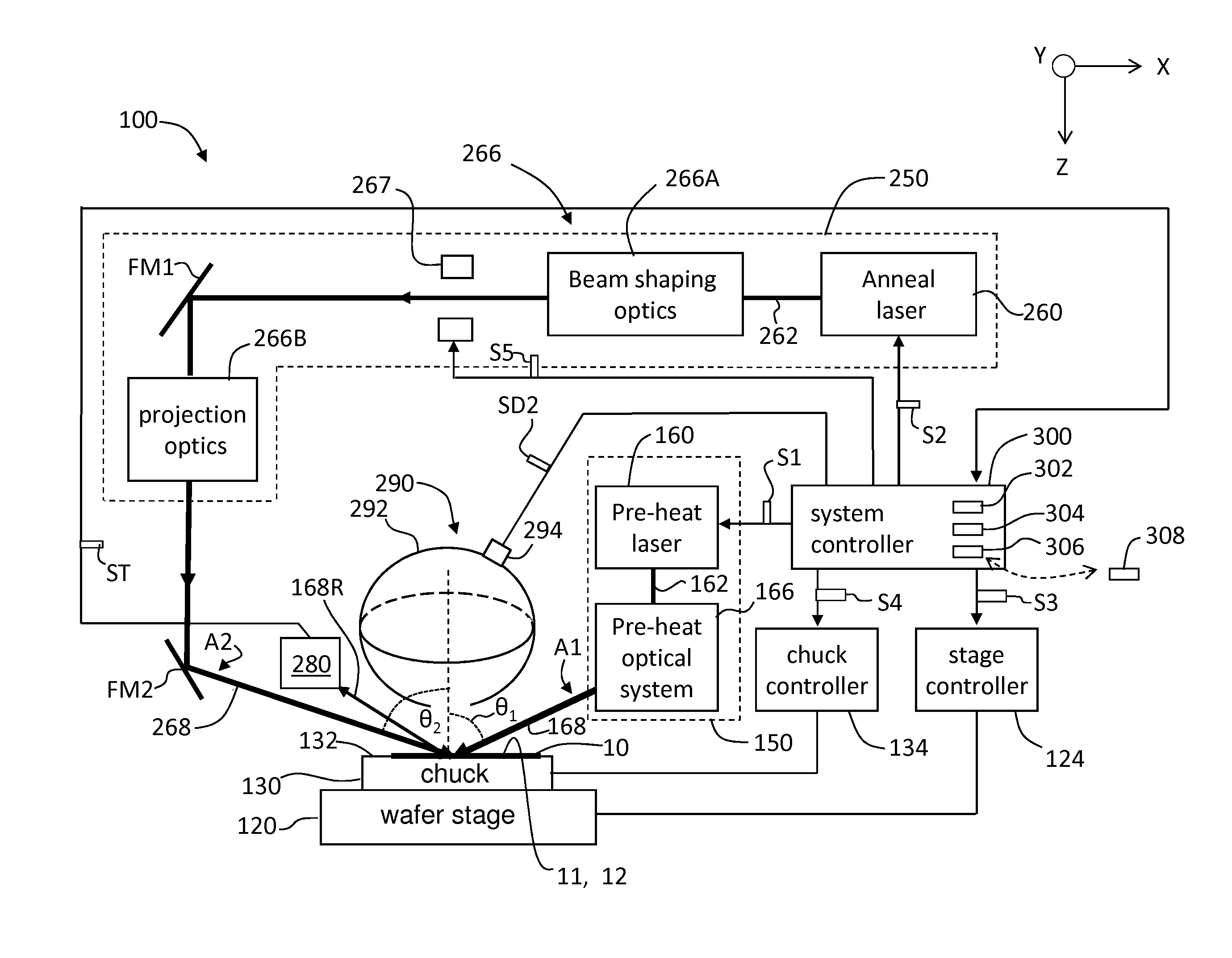
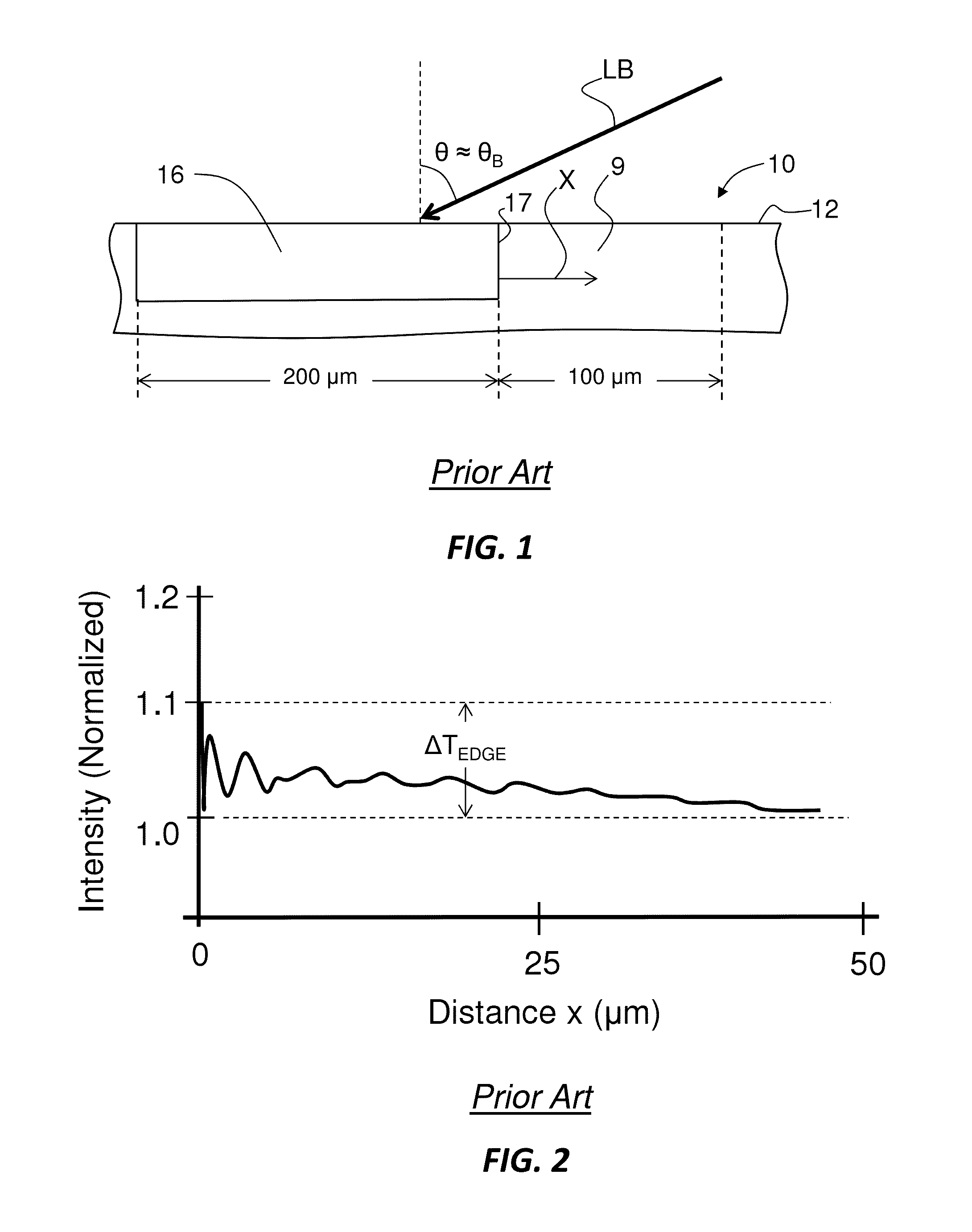
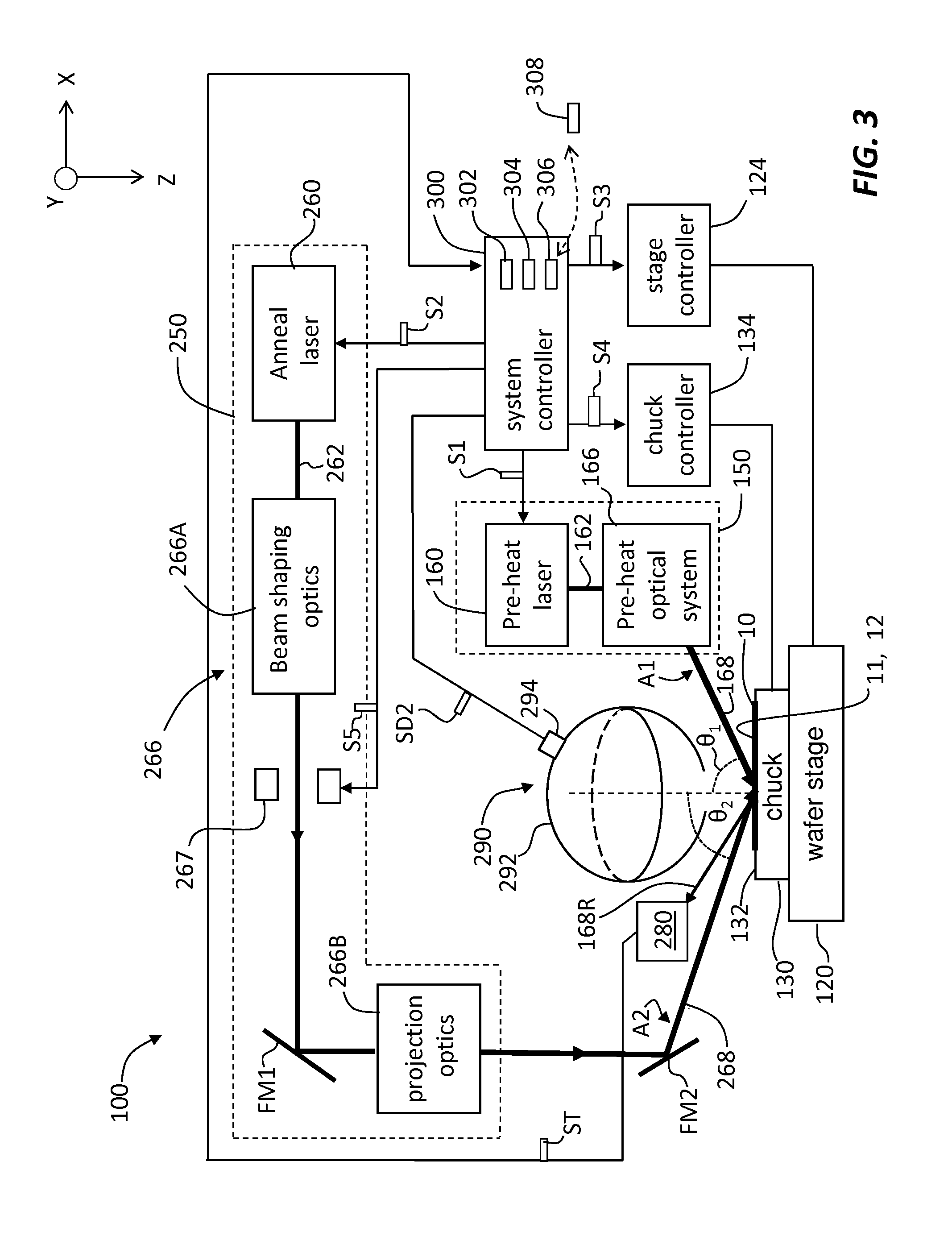
[0030]Reference is now made in detail to various embodiments of the disclosure, examples of which are illustrated in the accompanying drawings. Whenever possible, the same or like reference numbers and symbols are used throughout the drawings to refer to the same or like parts. The drawings are not necessarily to scale, and one skilled in the art will recognize where the drawings have been simplified to illustrate the key aspects of the disclosure. In some of the Figures, Cartesian coordinates are provided for the sake of reference and are not intended as providing limitations on specific directions and orientations of the systems and methods described herein. The claims as set forth below are incorporated into and constitute part of this detailed description.

[0031]In the discussion below, the term “semiconductor substrate” and “wafer” are synonymous and used interchangeably. Likewise, the terms “semiconductor wafer surface” and “wafer surface” are synonymous and used interchangeabl...


PUM

PropertyMeasurementUnit
surface temperatureaaaaaaaaaa
temperatureaaaaaaaaaa

Abstract

Systems and methods are disclosed for performing laser annealing in a manner that reduces or minimizes wafer surface temperature variations during the laser annealing process. The systems and methods include annealing the wafer surface with first and second laser beams that represent preheat and anneal laser beams having respective first and second intensities. The preheat laser beam brings the wafer surface temperate close to the annealing temperature and the anneal laser beam brings the wafer surface temperature up to the annealing temperature. The anneal laser beam can have a different wavelength, or the same wavelength but different orientation relative to the wafer surface. Reflectivity maps of the wafer surface at the preheat and anneal wavelengths are measured and used to select first and second intensities that ensure good anneal temperature uniformity as a function of wafer position.

Description

FIELD[0001]The present disclosure relates generally to annealing as used in semiconductor manufacturing to fabricate integrated circuits, and in particular relates to laser annealing of semiconductor wafers using two laser beams having different wavelengths to improve the temperature performance of the annealing process.BACKGROUND ART[0002]Millisecond laser annealing, such as laser spike annealing (LSA), has been widely adopted in advanced semiconductor device fabrication because it offers an ultra-low thermal budget, high dopant activation and super-abrupt junctions. A key challenge to implementing this type of annealing on patterned wafers is the potential large within-chip temperature non-uniformities that can arise from spatial variations in the optical and thermal properties of the wafer surface caused by the features of the IC chip. These adverse effects are referred to in the art as “pattern density effects” or just “pattern effects.”[0003]In one example of LSA, an infrared l...

Claims


Application Information

Patent Timeline
Patent Type & Authority Patents(United States)
IPC IPC(8): H01L29/04H01L31/036H01L31/20H01L31/0376
CPCG01N21/55H01L21/268H01L21/324H01L22/12H01L22/20H01L21/2636B23K26/0608B23K26/0732B23K26/08H01L2924/0002B23K2201/40H01L2924/00B23K2101/40
Inventor SHEN, XIAOHUAWANG, YUNWANG, XIAORU
Owner VEECO INSTR
Why Eureka
Try Eureka