Magneto-resistive effect element having spacer layer including gallium oxide layer with metal element
a technology of magnetoresistive effect and metal element, which is applied in the field of configuration of a spacer layer, can solve problems such as variation in ra
- Summary
- Abstract
- Description
- Claims
- Application Information
AI Technical Summary
Benefits of technology
Problems solved by technology
Method used
Image
Examples
first example
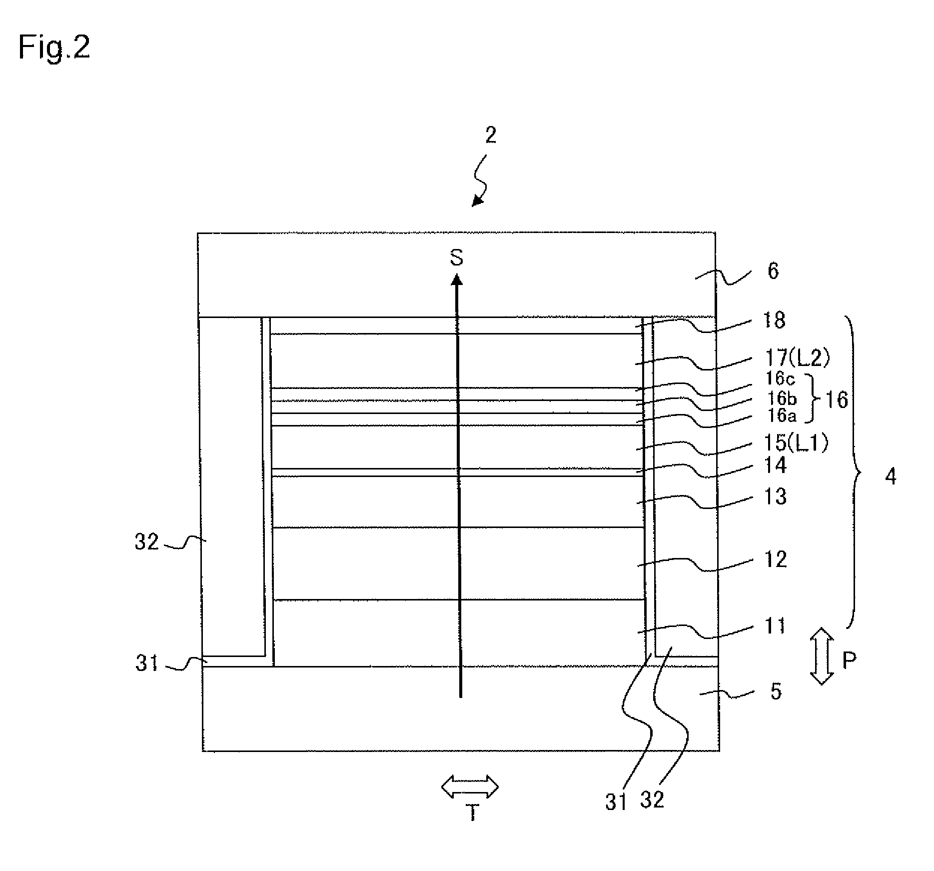
[0058]A multilayer film with the layer configuration illustrated in Table 1 was formed above a substrate W composed of Al2O3—TiC (ALTIC) by using a radio frequency (RF) sputtering device. Mg, Zn, In or Al was used as a metal element to add to a main spacer layer. In the present example, these elements were added as oxides. In the following explanation, oxides of Mg, Zn, In and Al are collectively referred to as MOx. The film thickness of the main spacer layer was 0.9 nm. The main spacer layer was formed by disposing a target composed of Ga2O3 and a target composed of MOx in a reaction chamber and colliding argon gas simultaneously with these targets. A target composed of Ga2O3 to which MOx was added may be used. Copper was used for the first nonmagnetic layer 16a and zinc was used for the second nonmagnetic layer 16c. After the film formation, heat treatment was performed at 250° C. for three hours. A plane size (junction size) of the MR element was 0.2 μm×0.2 μm.
[0059]In the above-...
second example
[0062]A multilayer film with a layer configuration illustrated in Table 2 was formed above a substrate W composed of Al2O3—TiC (ALTIC) by using a RF sputtering device. MgO, ZnO, In2O3 and Al2O3 were used as oxide metal MOx of a main spacer layer, and the film thickness of the main spacer layer was 0.9 nm. The main spacer layer was formed in the same process as the first example. Copper was used for a first nonmagnetic layer 116a and zinc was used for a second nonmagnetic layer 116c. After the film formation, heat treatment was performed at 250° C. for three hours. A plane size (junction size) of an MR element was 0.2 μm×0.2 μm.
[0063]As in the first example, the MR ratio, and the average value and variation of the RA were obtained by changing an atomic percent of Mg, Zn, In and Al. Table 5 and FIG. 6 illustrate the results.
[0064]
TABLE 5Main Spacer LayerMetalElementAtomicRA AverageRAGa2O3 +PercentNormalizedValueVariationSampleMox(At %)MR Ratio(Ωμm2)(%)#5-0No MOx01.000.2326.5added#5-1M...
PUM
| Property | Measurement | Unit |
|---|---|---|
| size | aaaaa | aaaaa |
| thickness | aaaaa | aaaaa |
| thickness | aaaaa | aaaaa |
Abstract
Description
Claims
Application Information


