
3D memory semiconductor device and structure

a semiconductor and 3d memory technology, applied in semiconductor devices, semiconductor/solid-state device details, electrical apparatus, etc., can solve the problems of many barriers to practical implementation of 3d stacked chips, copper or aluminum wiring levels, and wires (interconnects) that connect together transistors degrade in performance with scaling,

Inactive Publication Date: 2013-11-12
MONOLITHIC 3D
View PDF540 Cites 63 Cited by
  • Summary
  • Abstract
  • Description
  • Claims
  • Application Information

AI Technical Summary

Benefits of technology

This patent describes a way to create semiconductor chips that have wires and transistors arranged in a three-dimensional way to solve issues with wires in conventional chips. The invention aims to address challenges such as misalignment between wafers and low connectivity between layers in 3D stacked chips. The patent describes options for creating high-performance transistors at low temperatures, allowing for high-density connectivity despite misalignment, and designing a chip architecture that prevents degradation of the bottom transistors and wiring. The technical effects of this invention include improved performance, functionality, and power consumption of semiconductor chips.

Problems solved by technology

However, wires (interconnects) that connect together transistors degrade in performance with “scaling”.
However, there are many barriers to practical implementation of 3D stacked chips.
Copper or Aluminum wiring levels, in fact, can get damaged when exposed to temperatures higher than ˜400° C. If one would like to arrange transistors in 3 dimensions along with wires, it has the challenge described below.
When the Top Transistor Layer is constructed using Temperatures higher than 700° C., it can damage the Bottom Wiring Layer.Due to the above mentioned problem with forming transistor layers above wiring layers at temperatures lower than 400° C., the semiconductor industry has largely explored alternative architectures for 3D stacking In these alternative architectures, Bottom Transistor Layers, Bottom Wiring Layers and Contacts to the Top Layer are constructed on one silicon wafer.
Unfortunately, the size of Contacts to the other Layer is large and the number of these Contacts is small.
This low connectivity between layers is because of two reasons: (i) Landing pad size needs to be relatively large due to alignment issues during wafer bonding.
Etching deep holes in silicon with small lateral dimensions and filling them with metal to form TSVs is not easy.
Therefore, connectivity between two wafers is limited.
Unfortunately, however, almost all semiconductor devices in the market today (logic, DRAM, flash memory) utilize horizontal (or planar) transistors due to their many advantages, and it is difficult to convince the industry to move to vertical transistor technology.
A process flow is utilized to transfer this top transistor layer atop the bottom wiring and transistor layers at temperatures less than 400° C. Unfortunately, since transistors are fully formed prior to bonding, this scheme suffers from misalignment issues.
While Topol describes techniques to reduce misalignment errors in the above paper, the techniques of Topol still suffer from misalignment errors that limit contact dimensions between two chips in the stack to >130 nm.
Unfortunately, however, these technologies have higher defect density compared to standard single crystal silicon.
This higher defect density degrades transistor performance.
However, the approach described by Hubert has some challenges including the use of difficult-to-manufacture nanowire transistors, higher defect densities due to formation of Si and SiGe layers atop each other, high temperature processing for long times, and difficult manufacturing.

Method used


Image

  • 3D memory semiconductor device and structure
  • 3D memory semiconductor device and structure
  • 3D memory semiconductor device and structure

Examples


Embodiment Construction

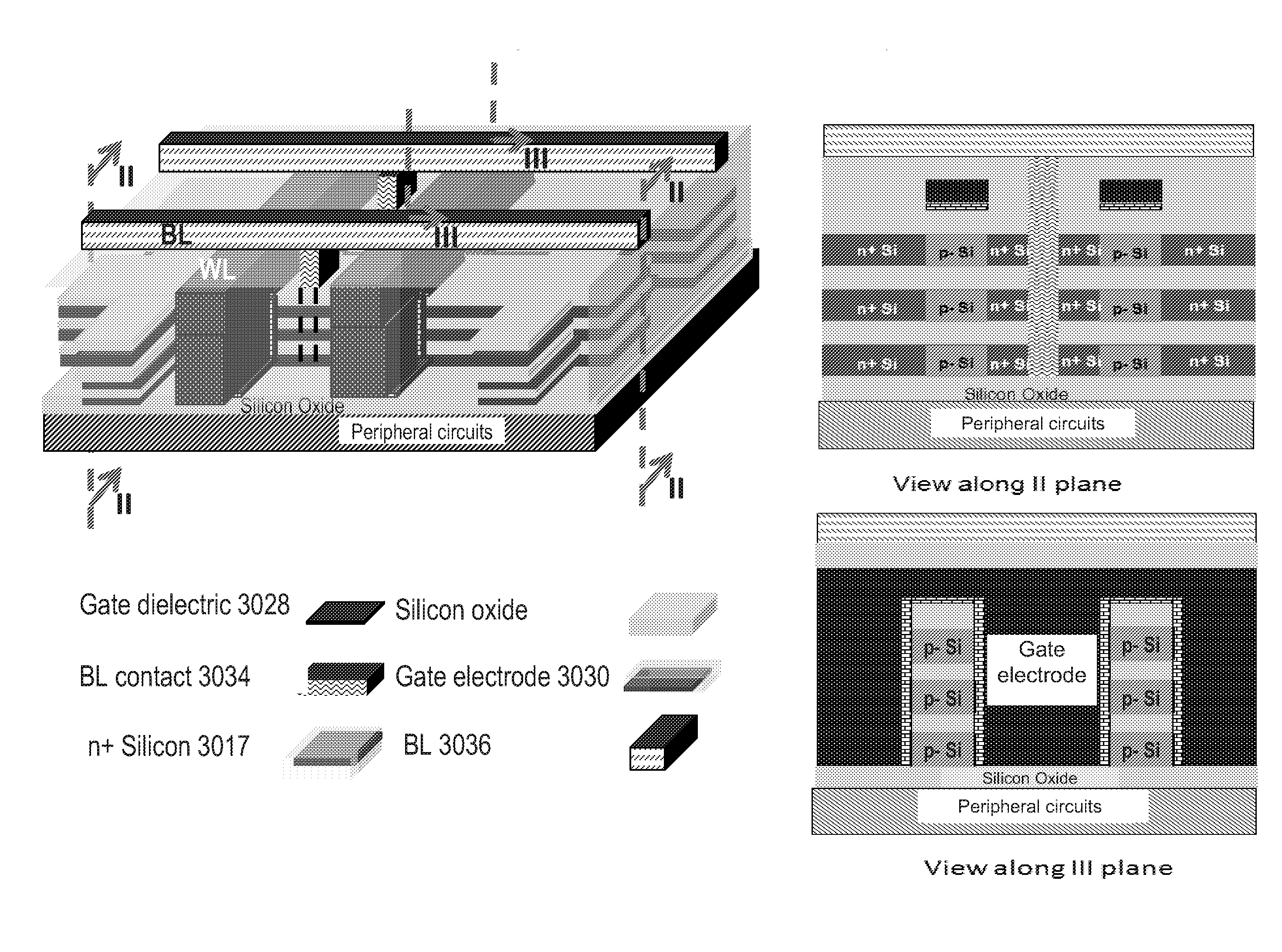
[0087]Embodiments of the present invention are now described with reference to FIGS. 1-52, it being appreciated that the figures illustrate the subject matter not to scale or to measure. Many figures describe process flows for building devices. These process flows, which are essentially a sequence of steps for building a device, have many structures, numerals and labels that are common between two or more adjacent steps. In such cases, some labels, numerals and structures used for a certain step's figure may have been described in previous steps' figures.

Section 1: Construction of 3D Stacked Semiconductor Circuits and Chips with Processing Temperatures Below 400° C.

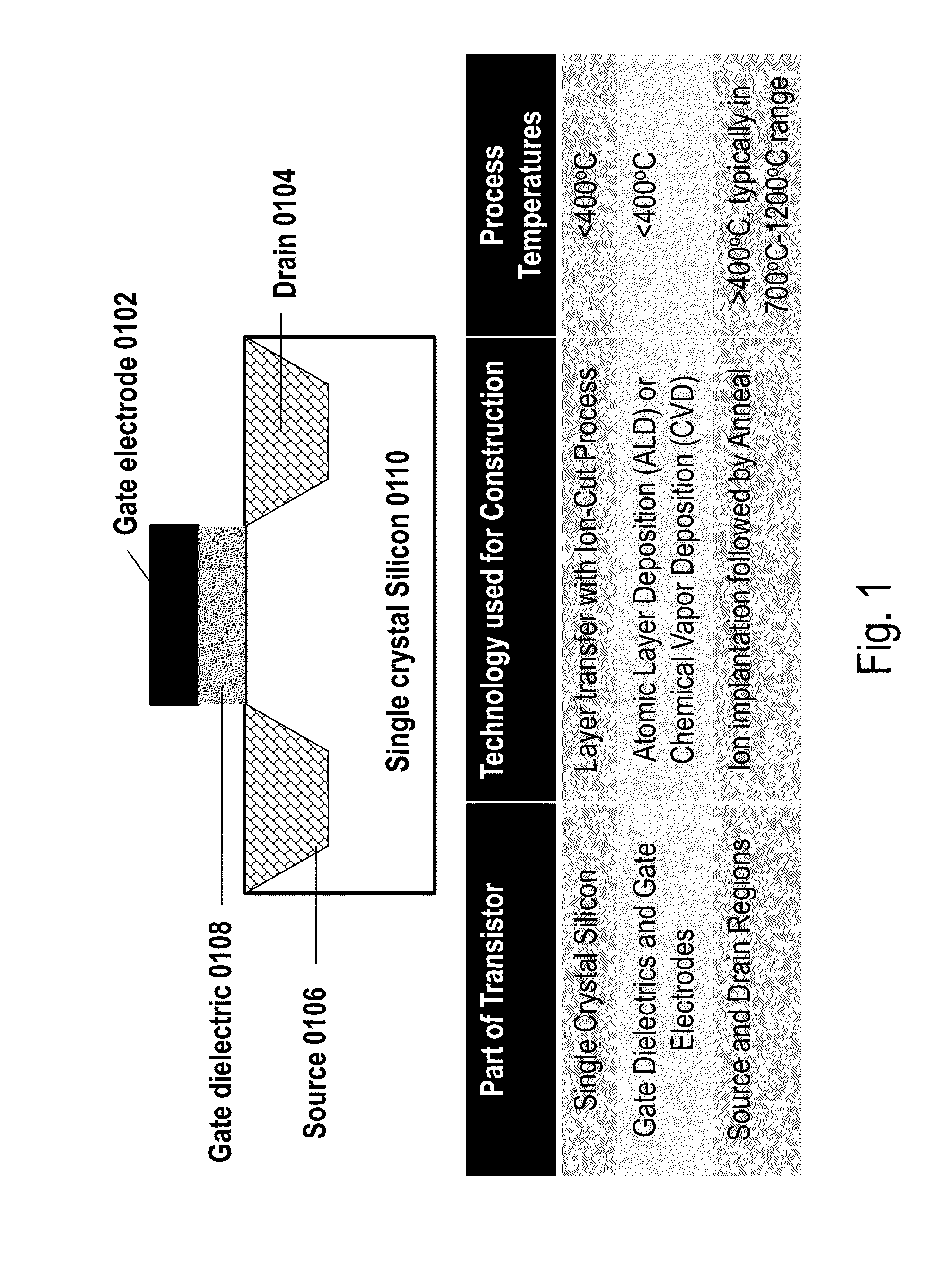
[0088]This section of the document describes a technology to construct single-crystal silicon transistors atop wiring layers with less than 400° C. processing temperatures. This allows construction of 3D stacked semiconductor chips with high density of connections between different layers, because the top-level transistor...


PUM


Abstract

A 3D memory device, including: a first memory layer including a first memory transistor with side gates; a second memory layer including a second memory transistor with side gates; and a periphery circuits layer including logic transistors for controlling the memory, the periphery circuits are covered by a first isolation layer, where the first memory layer includes a first monolithically mono-crystal layer directly bonded to a second isolation layer, and the second memory layer includes a second monolithically mono-crystal layer directly bonded to the second isolation layer, and the first mono-crystal layer is bonded on top of the first isolation layer, and the second memory transistor is self-aligned to the first memory transistor.

Description

[0001]This application claims priority of co-pending U.S. patent application Ser. Nos. 12 / 577,532, 12 / 706,520, 12 / 792,673, 12 / 847,911, 12 / 859,665, 12 / 903,862, 12 / 900,379, 12 / 901,890, 12 / 949,617, 12 / 970,602, 12,904,119, 12 / 951,913, and 13 / 016,313, the contents of which are incorporated by reference.BACKGROUND OF THE INVENTION[0002]1. Field of the Invention[0003]This invention describes applications of monolithic 3D integration to semiconductor chips performing logic and memory functions.[0004]2. Discussion of Background Art[0005]Over the past 40 years, one has seen a dramatic increase in functionality and performance of Integrated Circuits (ICs). This has largely been due to the phenomenon of “scaling” i.e. component sizes within ICs have been reduced (“scaled”) with every successive generation of technology. There are two main classes of components in Complementary Metal Oxide Semiconductor (CMOS) ICs, namely transistors and wires. With “scaling”, transistor performance and density ...

Claims


Application Information

Patent Timeline
IPC IPC(8): H01L29/78H01L23/535
CPCH01L29/78696H01L29/785H01L27/2436H01L27/249H01L21/84H01L27/0688H01L27/1203H01L27/0207H01L27/0694H01L27/092H01L23/544H01L21/6835H01L45/04H01L45/1226H01L2924/13062H01L2924/1461H01L2924/13091H01L45/146H01L27/10826H01L27/1108H01L27/11524H01L27/11582H01L2221/68327H01L2221/6834H01L2221/68363H01L2221/68381H01L2223/5442H01L2223/54426H01L2223/54453H01L2224/16H01L2224/73204H01L2924/15311H01L2924/00H01L2924/12032H01L2224/16225H01L2224/32225H10B63/30H10B63/845H10N70/20H10N70/823H10N70/8833H10B12/36H10B10/125H10B41/35H10B43/27
Inventor SEKAR, DEEPAK C.OR-BACH, ZVICRONQUIST, BRIAN
Owner MONOLITHIC 3D
Learn More