
Organic optoelectronic device coated with a multilayer encapsulation structure and a method for encapsulating said device

a multi-layer encapsulation and optoelectronic technology, applied in the direction of vacuum obtaining/maintenance, discharge tube luminescnet screens, gas-filled discharge tubes, etc., can solve the problems of degrading the cathode/organic film interface, not well suited to devices comprising flexible supports (e.g. flexible displays), and reducing permeability

Active Publication Date: 2014-01-28
COMMISSARIAT A LENERGIE ATOMIQUE ET AUX ENERGIES ALTERNATIVES
View PDF9 Cites 14 Cited by
  • Summary
  • Abstract
  • Description
  • Claims
  • Application Information

AI Technical Summary

Benefits of technology

The invention provides a device with an encapsulation structure that is thin and made up of organic layers. The structure is formed using a curable adhesive film that is exposed to vacuum, resulting in a thin and uniform film. The thickness of the encapsulation structure is significantly smaller than other methods, making it suitable for applications such as microdisplays. The process is faster and more efficient than other methods, and the resulting device has improved barrier properties and flexibility. The invention also provides a method for producing the inorganic layers that conform closely to microreliefs or nanoreliefs.

Problems solved by technology

This is because, if suitable protection is not in place, there is a risk that the device will subsequently degrade, which degradation manifests itself mainly through the appearance of black, non-emissive spots, in the case of OLEDs, which are in fact a result of water vapor penetrating into the diode, thereby degrading the cathode (or anode) / organic film interface.
Encapsulation with a cap is well suited to rigid devices, but it is not well suited to devices comprising flexible supports (e.g. flexible displays).
This encapsulation technique is also unfeasible in the case where space is lacking on the circuit of the substrate, for example in a CMOS (complementary metal-oxide semiconductor) microdisplay, and it is to be avoided if it is desired to minimize the weight of the device, in particular in the case of large emission areas.
Single inorganic layer encapsulation structures currently obtained using these PECVD or ALD techniques nevertheless have atmospheric gas impermeability properties that are unsatisfactory due to the defects that remain in these layers whatever is done.
A major drawback of multilayer structures comprising alternating organic and inorganic layers, such as Barix® structures, lies in the relatively large thickness (in general greater than 500 nm) of each polymer layer sandwiched between two inorganic layers, thereby leading to a large total thickness for the structure formed from n organic / inorganic dyads, in order to obtain the desired oxygen and water vapor impermeability properties.
Thus, for four of these dyads, it is easily possible to exceed a thickness of 2 μm, which is unfeasible for certain devices, such as microdisplays on CMOS substrates, which require very thin encapsulations.

Method used


Image

  • Organic optoelectronic device coated with a multilayer encapsulation structure and a method for encapsulating said device
  • Organic optoelectronic device coated with a multilayer encapsulation structure and a method for encapsulating said device

Examples


Embodiment Construction

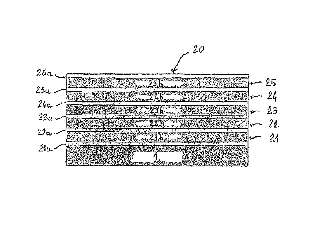
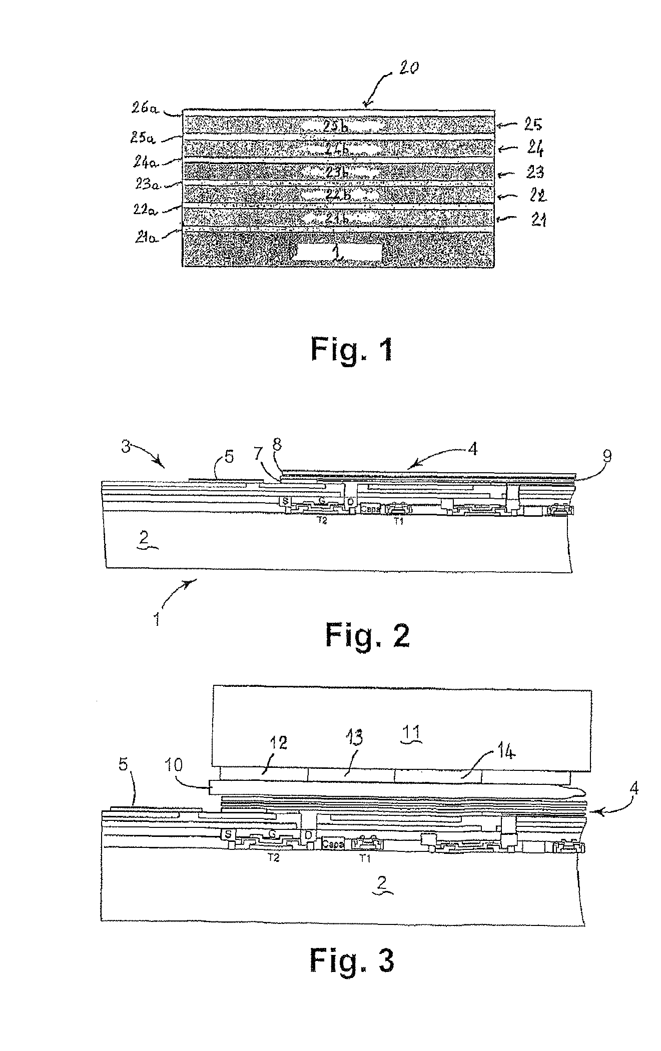
[0040]The multilayer encapsulation structure 20 illustrated in FIG. 1 covers the external side of an optoelectronic device 1 (e.g. the emission side of a light-emitting device 1), the sensitive components of which are to be protected from moisture and oxygen in the ambient air. This impermeable encapsulation structure 20 comprises five dyads 21 to 25 each consisting of a thin inorganic layer 21a to 25a coated with an organic layer, which forms a cured adhesive film 21b to 25b of reduced thickness and is sandwiched between two inorganic layers 21a and 22a, 22a and 23a, 23a and 24a, 24a and 25a, including the outermost organic layer 25b. In fact, the latter is covered by a thin external inorganic layer 26a which defines the exterior side of the encapsulation structure 20. It should be noted that these various layers in FIG. 1 are not shown at the scale of their respective thicknesses and lengths in the plane of the cross section.

[0041]The first internal dyad 21 of the structure 20 may...


PUM


Abstract

The invention relates to an organic optoelectronic device, such as a display, lighting or signalling device, that is protected from the ambient air by a sealed encapsulation in the form of a thin film, and to a method for encapsulating such a device. An optoelectronic device (1) according to the invention is coated with a sealed multi-layer encapsulation structure (20) comprising alternating inorganic layers (21a to 26a) and organic layers (21b to 25b). According to the invention, the device is such that at least one of said organic layers consists of a crosslinked adhesive film (21b to 25b) based on a glue that can be crosslinked thermally or by electromagnetic radiation, the or each adhesive film having a thickness uniformly lower than 200 n, said thickness being obtained by passing the film, which is deposited and not yet cross-linked, through a vacuum, such that the total thickness of the encapsulation structure is minimized.

Description

FIELD OF THE INVENTION[0001]The present invention relates to an organic optoelectronic device, such as a display, lighting or signaling device, which is protected from ambient air by an impermeable, thin-film encapsulation, and to a process for encapsulating such a device. The invention is applied for example to devices comprising organic light-emitting diodes (OLEDs), such as microscreens or microdisplays, to photovoltaic cells or else to organic thin-film transistors (TFTs), in a nonlimiting way.BACKGROUND OF THE INVENTION[0002]As is known, organic optoelectronic devices such as OLEDs, devices comprising photovoltaic cells, and those comprising organic TFTs, need to be encapsulated to protect their sensitive components from gaseous species in the atmosphere (mainly oxygen and water vapor). This is because, if suitable protection is not in place, there is a risk that the device will subsequently degrade, which degradation manifests itself mainly through the appearance of black, non...

Claims


Application Information

Patent Timeline
Patent Type & Authority Patents(United States)
IPC IPC(8): H01J1/62H05B44/00
CPCH01L2251/558H01L51/107H01L51/5237Y02E10/549H01L51/448H10K10/88H10K30/88H10K2102/351H10K59/8731H10K50/30H10K2102/302H10K50/8445
Inventor MAINDRON, TONYPRAT, CHRISTOPHE
Owner COMMISSARIAT A LENERGIE ATOMIQUE ET AUX ENERGIES ALTERNATIVES
Learn More