Semiconductor device

a semiconductor and on-state current technology, applied in the field of semiconductor devices, can solve the problems of large power consumption of on-state current, difficult manufacturing of transistors, and difficult manufacturing of semiconductor devices, and achieve the effects of reducing power consumption, increasing field-effect mobility and on-state current, and high speed

Active Publication Date: 2014-02-04
SEMICON ENERGY LAB CO LTD
View PDF155 Cites 23 Cited by
  • Summary
  • Abstract
  • Description
  • Claims
  • Application Information

AI Technical Summary

Benefits of technology

[0012]Thus, an object of an embodiment of the present invention is to provide a semiconductor device which can operate at high speed and consumes a smaller amount of power.
[0020]The transistors including oxide semiconductor films having different oxygen concentrations of the first regions overlapping with respective gate electrodes are manufactured. The transistor having higher oxygen concentration of the first region, i.e., the transistor including an oxide semiconductor film containing oxygen in a higher proportion than a proportion of oxygen in the stoichiometric ratio, includes a smaller number of oxygen defects in the oxide semiconductor film. Therefore, the donor level due to oxygen defects in the energy gap is low or does not substantially exist. As a result, leakage current is not easily generated in an off state, achieving a reduction in current at negative gate voltage of the transistor. On the other hand, since the transistor having lower oxygen concentration of the first region, i.e., the transistor including an oxide semiconductor film containing oxygen in a lower proportion than a proportion of oxygen in the stoichiometric ratio, includes oxygen defects, carriers are easily generated in an on state, resulting in an increase in field-effect mobility and on-state current of the transistor. Therefore, a semiconductor device which can operate at high speed and consume a smaller amount of power can be manufactured by formation of transistors in accordance with characteristics of circuits included in the semiconductor device. Specifically, a transistor having high field-effect mobility and large on-state current is used in a circuit which needs to operate at high speed and a transistor having small current at negative gate voltage is used in a circuit with small leakage current.
[0021]According to an embodiment of the present invention, a transistor including a large number of oxygen defects in an oxide semiconductor film and a transistor including a small number of oxygen defects in an oxide semiconductor film can be manufactured. As a result, a transistor having high field-effect mobility and large on-state current and a transistor having small current at negative gate voltage can be manufactured. Further, these transistors are separately formed in circuits in accordance with functions thereof, whereby a semiconductor device can operate at high speed and consume a smaller amount of power.

Problems solved by technology

It is difficult to manufacture a transistor including an oxide semiconductor which has all characteristics of small current at negative gate voltage, high field-effect mobility, and large on-state current.
A semiconductor device including a transistor having high field-effect mobility and large on-state current consumes a large amount of power due to the current of the transistor at negative gate voltage.
In contrast, it is difficult for a semiconductor device including a transistor having small current at negative gate voltage to operate at high speed because the transistor has low field-effect mobility and small on-state current.

Method used


Image

  • Semiconductor device
  • Semiconductor device
  • Semiconductor device

Examples


embodiment 1

(Embodiment 1)

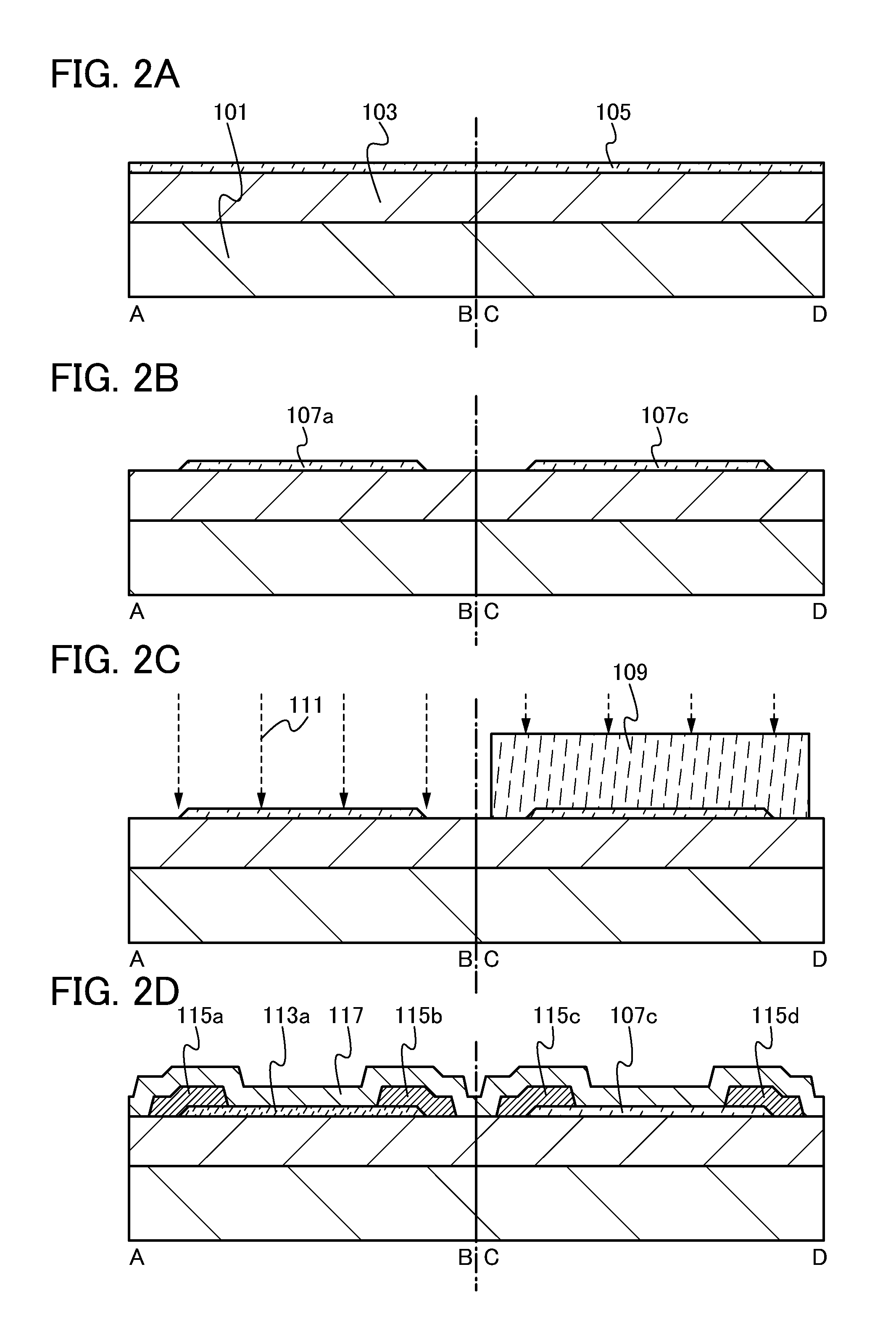
[0049]In this embodiment, a structure of a semiconductor device including a transistor having small current at negative gate voltage and a transistor having high field-effect mobility and large on-state current, and a method for manufacturing the semiconductor device will be described with reference to FIG. 1, FIGS. 2A to 2D, and FIGS. 3A to 3C. The transistors of this embodiment are each a coplanar transistor having a top gate structure and are each characterized in that a pair of electrodes covers side surfaces and part of a top surface of an oxide semiconductor film.

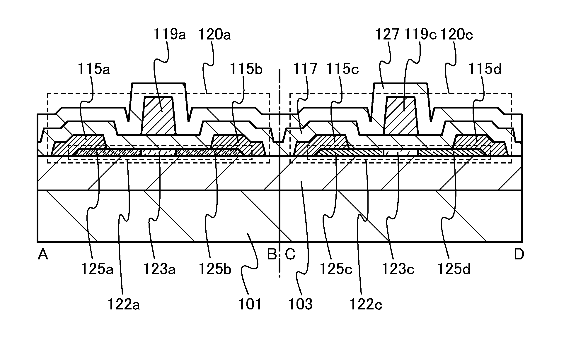
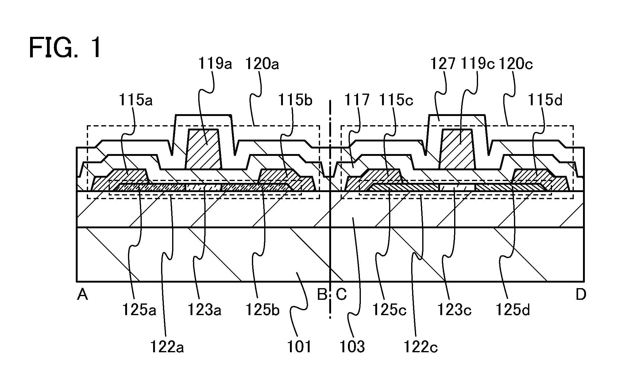
[0050]FIG. 1 is a cross-sectional view of the semiconductor device described in this embodiment. The semiconductor device illustrated in FIG. 1 includes a transistor 120a having small current at negative gate voltage and a transistor 120c having high field-effect mobility and large on-state current.

[0051]The transistor 120a having small current at negative gate voltage includes an insulating film 103 ove...

embodiment 2

(Embodiment 2)

[0170]In this embodiment, a transistor having a structure different from that of Embodiment 1 and a method for manufacturing the transistor will be described with reference to FIGS. 2A to 2D, FIG. 4, and FIGS. 5A to 5C. Coplanar transistors each having a top gate structure are described in this embodiment.

[0171]FIG. 4 is a cross-sectional view of a semiconductor device described in this embodiment. The semiconductor device illustrated in FIG. 4 includes a transistor 130a having small current at negative gate voltage and a transistor 130c having high field-effect mobility and large on-state current.

[0172]The transistor 130a having small current at negative gate voltage includes the insulating film 103 over the substrate 101, the oxide semiconductor film 122a over the insulating film 103, the gate insulating film 117 covering the oxide semiconductor film 122a, and the gate electrode 119a which is provided over the gate insulating film 117 and overlaps with the oxide semi...

embodiment 3

(Embodiment 3)

[0188]In this embodiment, a transistor having a structure different from the structures of Embodiments 1 and 2 and a method for manufacturing the transistor will be described with reference to FIGS. 2A to 2D, FIG. 6, FIGS. 7A to 7C, and FIGS. 8A to 8C. The transistor described in this embodiment includes an oxide semiconductor film having a structure different from that in Embodiment 1.

[0189]FIG. 6 is a cross-sectional view of a semiconductor device described in this embodiment. The semiconductor device illustrated in FIG. 6 includes a transistor 150a having small current at negative gate voltage and a transistor 150c having high field-effect mobility and large on-state current.

[0190]The transistor 150a having small current at negative gate voltage includes the insulating film 103 over the substrate 101, an oxide semiconductor film 146a over the insulating film 103, the pair of electrodes 115a and 115b which is in contact with the oxide semiconductor film 146a and serv...


PUM


Abstract

A semiconductor device which can operate at high speed and consumes a smaller amount of power is provided. In a semiconductor device including transistors each including an oxide semiconductor, the oxygen concentration of the oxide semiconductor film of the transistor having small current at negative gate voltage is different from that of the oxide semiconductor film of the transistor having high field-effect mobility and large on-state current. Typically, the oxygen concentration of the oxide semiconductor film of the transistor having high field-effect mobility and large on-state current is lower than that of the oxide semiconductor film of the transistor having small current at negative gate voltage.

Description

BACKGROUND OF THE INVENTION[0001]1. Field of the Invention[0002]The present invention relates to a semiconductor device which includes a circuit including a semiconductor element such as a transistor, and a method for manufacturing the semiconductor device. For example, the present invention relates to a power device which is mounted on a power supply circuit; a semiconductor integrated circuit including a memory, a thyristor, a converter, an image sensor, or the like; an electro-optical device typified by a liquid crystal display panel; a light-emitting display device including a light-emitting element; and an electronic device including any of the above as a component.[0003]In this specification, a semiconductor device means all types of devices which can function by utilizing semiconductor characteristics, and an electro-optical device, a light-emitting display device, a semiconductor circuit, and an electronic device are all semiconductor devices.[0004]2. Description of the Rela...

Claims


Application Information

Patent Timeline
Patent Type & Authority Patents(United States)
IPC IPC(8): H01L29/10H01L29/18H01L27/148
CPCH01L27/1225H01L29/04H01L29/06H01L29/7869
Inventor YAMAZAKI, SHUNPEIYAMADE, NAOTOKOEZUKA, JUNICHI
Owner SEMICON ENERGY LAB CO LTD
Why Eureka
Try Eureka