Supercharge Your Innovation With Domain-Expert AI Agents!

Image compression circuit for compressing pieces of image data of four adjacent pixels, image compression method, semiconductor device, and smartphone

a compression circuit and image data technology, applied in the field of image compression circuits, can solve the problems of degrading the the inability to ensure the memory capacity of the display driver, and the inability to store image data of one frame, so as to achieve the effect of suppressing the degrading image quality of the compressed image data without reducing the compression rate of image data

Inactive Publication Date: 2014-02-18
ROHM CO LTD
View PDF7 Cites 0 Cited by
  • Summary
  • Abstract
  • Description
  • Claims
  • Application Information

AI Technical Summary

Benefits of technology

The adaptive compression system effectively suppresses image quality degradation while maintaining high compression rates by selectively using RGB or YCbCr compression methods based on pixel variations, ensuring efficient memory usage and improved image processing capabilities.

Problems solved by technology

In the case that there is a restriction to a chip size of the display driver, the capacity of the memory of the display driver cannot be ensured, and the image data of one frame cannot be stored.
However, unfortunately the image quality of the compressed image data is degraded when the image compression circuit simply compresses the image data by converting the image data of each pixel expressed by the RGB color space into the image data of each pixel expressed by the YCbCr color space.
In the image compression circuit, there is also a problem in that a compression rate of the image data is lowered to increase the information amount of the compressed image data when the degradation of the image quality of the compressed image data is suppressed.

Method used


Image

  • Image compression circuit for compressing pieces of image data of four adjacent pixels, image compression method, semiconductor device, and smartphone
  • Image compression circuit for compressing pieces of image data of four adjacent pixels, image compression method, semiconductor device, and smartphone
  • Image compression circuit for compressing pieces of image data of four adjacent pixels, image compression method, semiconductor device, and smartphone

Examples


first embodiment

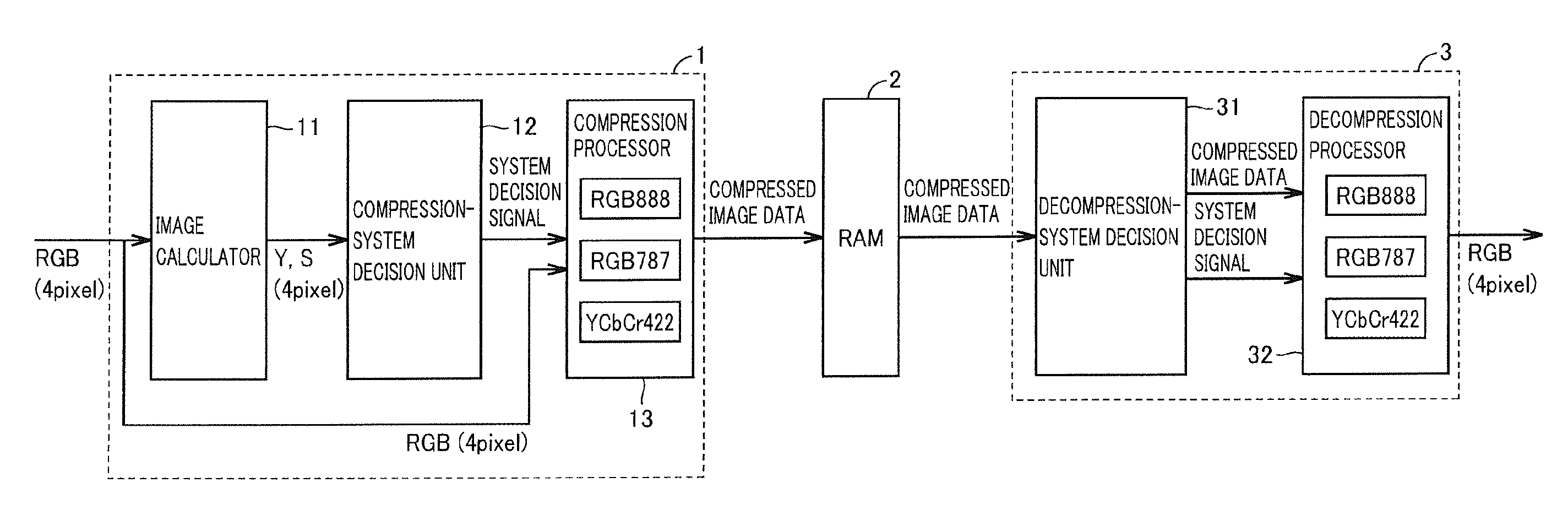
[0029]FIG. 1 is a block diagram illustrating a configuration of an image compression circuit according to a first embodiment of the invention. An image compression circuit 1 of the first embodiment in FIG. 1 compresses pieces of image data of four adjacent pixels. Examples of the four adjacent pixels include four pixels that are arrayed in a 2-by-2 matrix form and four pixels that are consecutively arrayed in a row direction. In the following embodiments, the four adjacent pixels are described as the four pixels that are arrayed in the 2-by-2 matrix form.

[0030]In addition to image compression circuit 1, FIG. 1 also illustrates a memory (RAM: Random Access Memory) 2 in which the compressed image data compressed by image compression circuit 1 is stored and an image decompression circuit 3 that takes out the compressed image data stored in memory 2 and decompresses the taken-out compressed image data. Image compression circuit 1 and image decompression circuit 3 may be configured by so...

second embodiment

[0073]Because a configuration of an image compression circuit according to a second embodiment of the invention is identical to that of image compression circuit 1 of the first embodiment in FIG. 1, the detailed description thereof is not repeated. In the following description, each component of the image compression circuit of the second embodiment is designated by the same reference as image compression circuit 1 of the first embodiment. FIG. 6 is a flowchart illustrating an operation of an image compression circuit 1 according to a second embodiment of the invention.

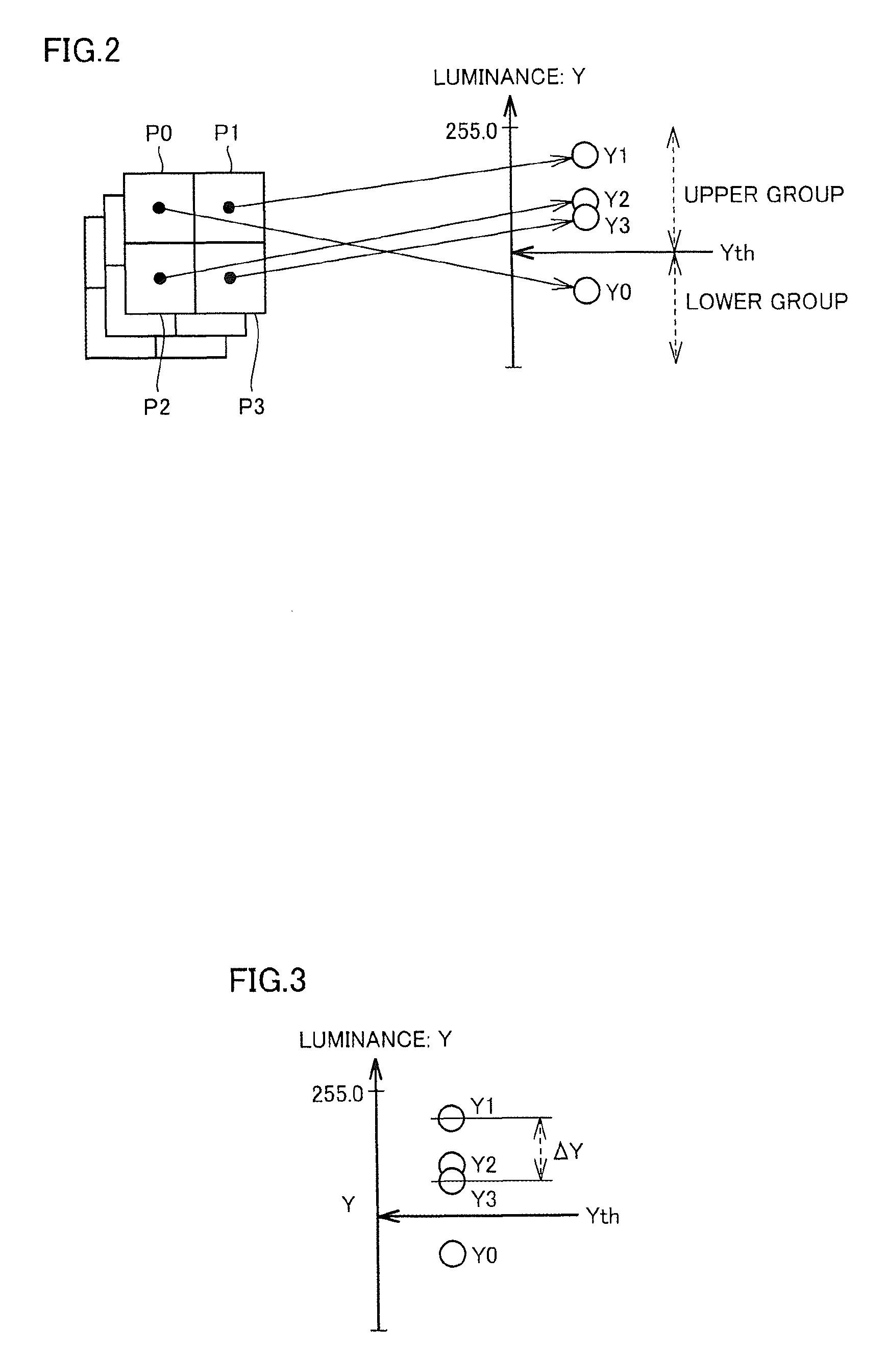
[0074]Image calculator 11 calculates luminance Y and color differences Cb, Cr, and Cg of each pixel from four-pixel image data expressed by the RGB color space (Step S61). Specifically, assuming that red (RED), green (GREEN), and blue (BLUE) are the color components of the image data, luminance Y can be calculated using the conversion equation given by equation 1, and color differences Cb, Cr, and Cg can be calculated...

third embodiment

[0088]FIG. 10 is a block diagram illustrating a configuration of a semiconductor device according to a third embodiment of the invention. For example, a semiconductor device 100 in FIG. 10 is a display driver that displays the image on a liquid crystal display device. Semiconductor device 100 includes image compression circuit 1, memory 2, and image decompression circuit 3 of the first or second embodiment. Semiconductor device 100 also includes a frame memory 4, a line buffer 5, a register 6, a FIFO (first-in first-out) circuit 7, a data comparison circuit 8, and an image processing circuit 9.

[0089]Frame memory 4 retains the input image data in units of frames. Line buffer 5 temporarily retains the image data, which is processed by image compression circuit 1, in units of lines. Register 6 retains setting information on image compression circuit 1. FIFO circuit 7 stores the compressed image data compressed by image compression circuit 1 in memory 2 in a first-in first-out manner, a...


PUM


Abstract

An image compression circuit 1 of the invention includes an image calculator 11, a compression-system decision unit 12, and a compression processor 13. Compression-system decision unit 12 determines a variation of pieces of image data of four adjacent pixels based on a variation in luminance Y of the pixels or variations in luminance Y and saturation S of the pixels, compresses the image data into image data of one or two pixels (RGB 888 and RGB 787) expressed by an RGB color space having a small quantization error in the case of the small variation of the pieces of image data, and compresses the image data into data including the luminances of the four adjacent pixels and pieces of image data of two pixels (YCbCr 422) expressed by a YCbCr color space having a large quantization error in the case of the large variation of the pieces of image data.

Description

BACKGROUND OF THE INVENTION[0001]1. Field of the Invention[0002]The present invention relates to an image compression circuit, an image compression method, a semiconductor device, and a smartphone, particularly to an image compression circuit for compressing pieces of image data of four adjacent pixels, an image compression method, a semiconductor device, and a smartphone.[0003]2. Description of the Related Art[0004]Recently, in a display device, an amount of information on image data to be processed increases with increasing resolution of an image, and sometimes image processing of comparing the image data of a preceding frame and the image data of a current frame is performed in order to improve image quality of a moving image. Therefore, in order to perform the image processing of comparing the image data of the preceding frame and the image data of the current frame, it is necessary that a display driver that displays the image on the display device include a memory in which the...

Claims


Application Information

Patent Timeline
Patent Type & Authority Patents(United States)
IPC IPC(8): G06K9/00H04N1/41H04N19/00H04N19/12H04N19/134H04N19/136H04N19/182H04N19/186H04N19/189H04N19/196H04N19/46H04N19/50H04N19/70
CPCH04N19/00278H04N19/00012H04N19/0009H04N19/00884H04N19/00157H04N19/176H04N19/14H04N19/124H04N19/70H04N19/102
Inventor YAMAMOTO, TAKATERU
Owner ROHM CO LTD
Features
  • R&D
  • Intellectual Property
  • Life Sciences
  • Materials
  • Tech Scout
  • Unparalleled Data Quality
  • Higher Quality Content
  • 60% Fewer Hallucinations
Learn More