Light emitting panel device wherein a plurality of panels respectively having light emitting sections are connected, and image display device and illuminating device provided with the light emitting panel device

a technology of light emitting panel and image display device, which is applied in the direction of solid-state devices, organic semiconductor devices, thermoelectric devices, etc., can solve the problems of low processing increase in the size of shadow mask, and low alignment accuracy of shadow mask, so as to achieve the effect of providing the image display device at low cost and low cos

Active Publication Date: 2014-03-18
SHARP KK
View PDF26 Cites 7 Cited by
  • Summary
  • Abstract
  • Description
  • Claims
  • Application Information

AI Technical Summary

Benefits of technology

[0036]As described above, a light-emitting panel device of the present invention includes: a plurality of panels each having a rectangular light-emitting section in which a plurality of light-emitting elements are arranged on a flat surface of a base, each of the plurality of light-emitting elements (i) having a first electrode and a second electrode, and (ii) emitting light by being supplied with a current or a voltage, the base being curved or bent at one of two edge parts of the flat surface of the base so as to provide an adjacent surface which (I) projects on a side opposite to a flat surface side and (II) is adjacent to the one of two edge parts of the flat surface, the two edge parts extending along a pair of long sides constituting the rectangular light-emitting section, respectively, the adjacent surface being provided with a group of terminals thereon, which extend from the first electrode of each of the plurality of light-emitting elements of the rectangular light-emitting section, adjacent ones of the plurality of panels being combined with each other in such a manner that (1) a rectangular light-emitting section of one of the plurality of panels and a rectangular light-emitting section of an adjacent one of the plurality of panels are arranged to face in an identical direction, and (2) one of edge parts of a flat surface of a base of the one of the plurality of panels and one of edge parts of a flat surface of a base of the adjacent one of the plurality of panels are coupled together so that a longitudinal direction of the rectangular light-emitting section of the one of the plurality of panels and a longitudinal direction of the rectangular light-emitting section of the adjacent one of the plurality of panels are parallel to each other.
[0037]With the arrangement, it is possible that (i) there is no limitation in the number of the plurality of panels thus combined (connected), (ii) a problem of connection parts between the plurality of panels are solved, and (iii) even in a case where a large panel is manufactured, a size of each of the plurality of panels can be reduced to a desired area so that a desired compact panel is obtained.
[0038]Further, an image display device of the present invention includes the light-emitting panel device. It is therefore possible to (i) cause the image display device to be larger than a conventional arrangement and (ii) provide the image display device at low cost. Furthermore, an illumination device of the present invention includes the light-emitting panel device. It is therefore possible to (i) cause the illumination device to be larger than a conventional arrangement and (ii) provide the illumination device at low cost.

Problems solved by technology

This method, however, has problems of low processing accuracy of the shadow mask, low alignment accuracy of the shadow mask, and an increase in the size of the shadow mask.
Accordingly, it is difficult to manufacture a large mask.
Further, the conventional method also has problems in manufacturing and processing a mask in accordance with a large substrate.
Low processing accuracy and low alignment accuracy cause light-emitting layers to be mixed with each other (i.e., a mixture of colors).
Such a reduction in aperture ratio results in a reduction in luminance, an increase in power consumption, and a reduction in a lifetime of the display.
With the method, however, the larger the substrate (the mask) becomes, the greater a flexure of the mask becomes in a center of the substrate.
The problem of the flexure also causes the mixture of colors.
Further, there is a case where the substrate has a part where no organic layer is provided due to significant flexure of the mask.
This causes a leakage of a current between electrodes, and such a leakage results in a defect of the display.
In addition, according to the conventional method, when the mask is used a certain number of times, the mask is deteriorated.
It is impossible to use the mask thus deteriorated.
Accordingly, the larger the mask becomes, the higher a production cost of the display becomes.
The increase in production cost is regarded as the biggest problem in the field of the organic EL display.
This reduces display quality of the display.

Method used


Image

  • Light emitting panel device wherein a plurality of panels respectively having light emitting sections are connected, and image display device and illuminating device provided with the light emitting panel device
  • Light emitting panel device wherein a plurality of panels respectively having light emitting sections are connected, and image display device and illuminating device provided with the light emitting panel device
  • Light emitting panel device wherein a plurality of panels respectively having light emitting sections are connected, and image display device and illuminating device provided with the light emitting panel device

Examples


example 1

Image Display Device

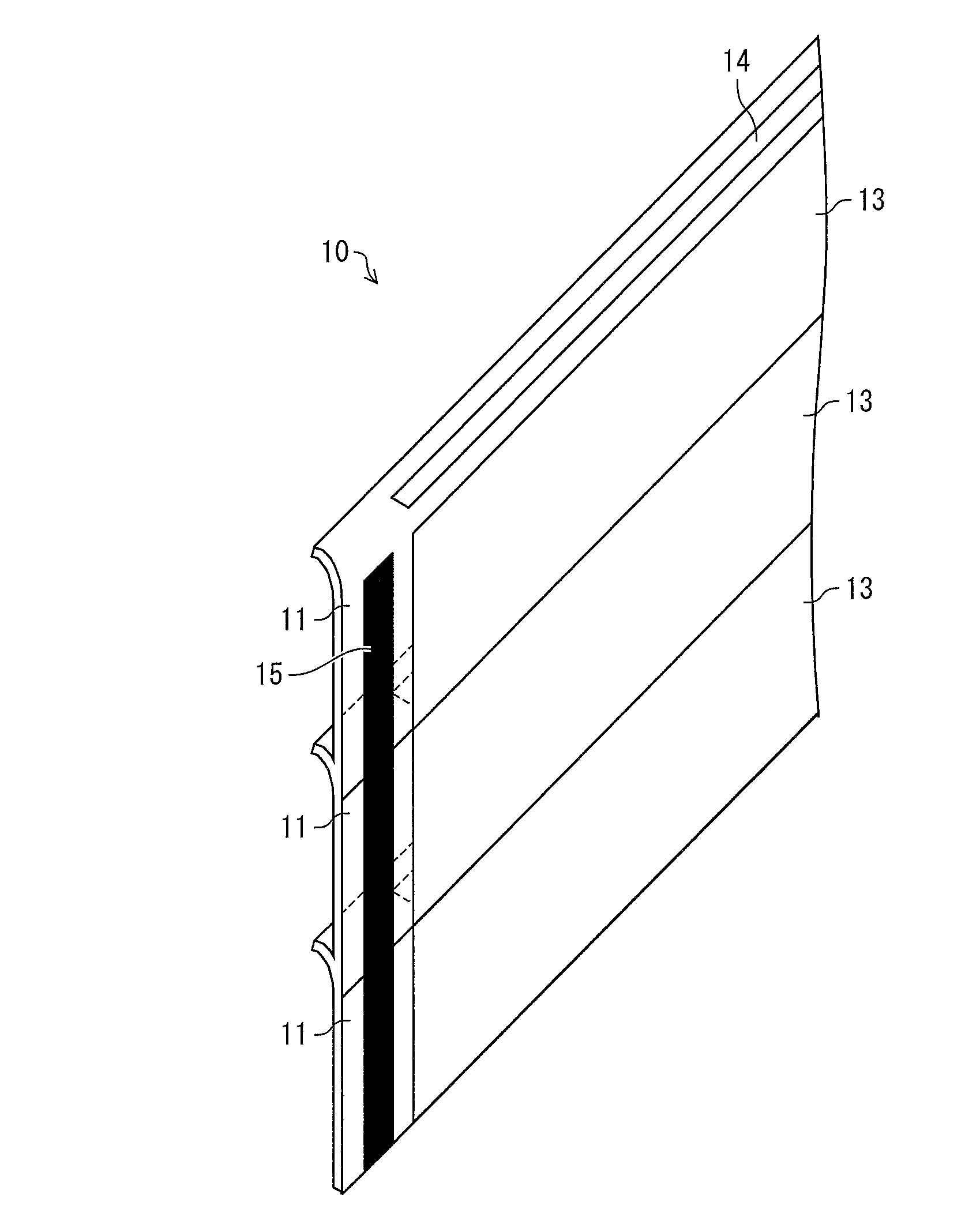
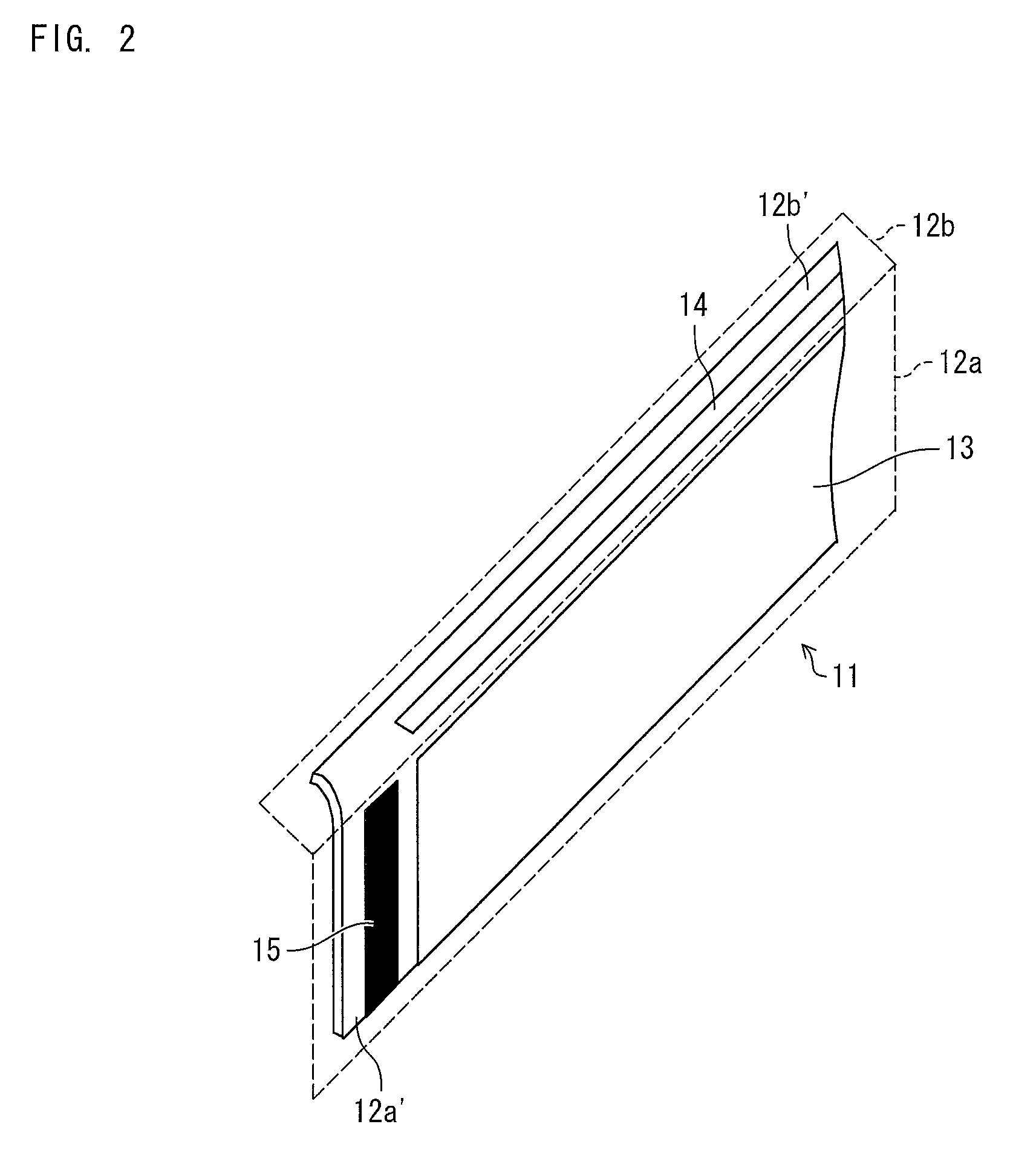
[0229]As a substrate 12 (see FIG. 2), a plastic substrate coated with silicon oxide (thickness: 200 nm) was employed. The plastic substrate had a thickness of 0.2 mm, and had a surface having an area of 500 mm×220 mm.

[0230]On the surface of the plastic substrate 12, indium-tin oxide (ITO) was provided by a sputtering method so that the surface had a resistance of 10Ω / □. As a result, a transparent electrode (anode), having a film thickness of 200 nm was formed. The transparent electrode was to serve as a first electrode 20.

[0231]Next, patterning was carried out by a photolithography method with respect to only a region of 492 mm×220 mm in the surface of 500 mm×220 mm, so as to form the first electrode 20 (see FIG. 4). The first electrode 20 had a stripe pattern having a length of 250 mm and a width of 1 mm.

[0232]Next, in order to form an edge cover on an edge part of the first electrode 20, SiO2 (thickness: 200 nm) was provided. Then, patterning was carried out by...

example 2

Illumination Device

[0250]As a substrate 12 (see FIG. 2), a plastic substrate coated with a silicon oxide (thickness: 0.2 mm) was employed. The plastic substrate had a surface having an area of 500 mm×220 mm and had a thickness of 0.2 mm.

[0251]On the surface of the plastic substrate 12, indium-tin oxide (ITO) was provided by a sputtering method so that the surface has a resistance of 10Ω / □. A transparent electrode (anode) having a film thickness of 300 nm was thus formed. The transparent electrode was to serve as a first electrode 20.

[0252]Next, patterning was carried out by a photolithography method with respect to only a region of 492 mm×216 mm in the surface of 500 mm×220 mm, so that the ITO was left and therefore the first electrode 20 (see FIG. 4) was formed.

[0253]Next, in order to form an edge cover on an edge part of the first electrode 20, SiO2 was provided by the sputtering method so that an SiO2 layer having a thickness of 200 nm was provided. Then, patterning was carried o...

example 3

Active Driving Organic El Image Display Device

[0267]As a substrate 12 (see FIG. 2), a substrate made from an invar material, coated with silicon oxide (thickness: 10 μm), was employed. The substrate had a thickness of 0.1 mm, and had a surface having an area of 750 mm×220 mm.

[0268]On a glass substrate, an amorphous silicon semiconductor film was formed by a PECVD method. Then, a crystallizing process was carried out so as to form a polycrystalline silicon semiconductor film. Next, patterning was carried out by use of a photolithography method so that a plurality of island shapes of the polycrystalline silicon semiconductor film were formed. Then, on the polycrystalline silicon semiconductor layer thus patterned, the gate insulating film and the gate electrode layer were formed in this order, and after that, patterning was carried out by use of the photolithography method.

[0269]After that, the polycrystalline semiconductor film thus patterned was doped with an impurity element such a...


PUM


Abstract

Panel (11) of the present invention includes substrate (12) having flat surface (12a′) having rectangular display section (13), and adjacent surface (12b′) curved from an edge part of surface (12a′) in the vicinity of a long side of surface (12a′). On surface (12b′), terminals, extending from display section (13) (in the vicinity of the long side), are arranged. Edge parts of surfaces (12a′) of substrates (12) of adjacent panels (11) are combined so that longitudinal directions of light-emitting sections (13) are parallel to each other. Surface (12b′) projects on a back surface side of substrate (12). It is thus possible to provide a light-emitting panel device realizing a large light-emitting surface by combining a desired number of panels, an image display device including the light-emitting panel device, an illumination device including the light-emitting panel device, a panel in the light-emitting panel device, and a method of producing the panel.

Description

CROSS REFERENCE TO RELATED APPLICATIONS[0001]This is a U.S. National Phase patent application of PCT / JP2010 / 058560, filed May 20, 2010, which claims priority to Japanese Patent Application No. 2009-234346, filed Oct. 8, 2009, each of which is hereby incorporated by reference in the present disclosure in its entirety.TECHNICAL FIELD[0002]The present invention relates to: a light-emitting panel device in which a plurality of panels each having a light-emitting section are connected to each other; an image display device including the light-emitting panel device; and an illumination device including the light-emitting panel device. More specifically, the present invention relates to: an image display device having a large-screen organic EL display which is realized by causing a plurality of panels, each having an organic electroluminescence (EL) element in a display section, to be connected to each other; and an illumination device including the organic EL display.BACKGROUND ART[0003]I...

Claims


Application Information

Patent Timeline
Patent Type & Authority Patents(United States)
IPC IPC(8): H01L27/14
CPCH01L51/50H01L51/5203H01L27/3276H01L2251/5361H01L27/3293H10K59/18H10K59/131H10K50/00H10K50/805
Inventor FUJITA, YOSHIMASAOGATA, HIDENORIOKAMOTOKOBAYASHI, YUHKIYAMADA, MAKOTO
Owner SHARP KK
Why Eureka
Try Eureka