Aqueous, acid bath and method for the electrolytic deposition of copper

a technology of electrolysis and copper, applied in the field of acid bath and method for electrolysis deposition of copper, can solve the problems of difficult uniform deposition of copper in view of geometric arrangement, rejection of the entire printed circuit board or chip carrier, and inability to meet the requirements of the electrolytic process, so as to limit the roughness of deposited copper and facilitate the drilling of holes through the copper foil

Active Publication Date: 2014-03-25
ATOTECH DEUT GMBH
View PDF17 Cites 14 Cited by
  • Summary
  • Abstract
  • Description
  • Claims
  • Application Information

AI Technical Summary

Benefits of technology

[0004]U.S. Pat. No. 2,876,178 describes an alkaline cyanide copper bath in which amino acids or secondary amino acid derivatives, such as peptones and peptides, are contained. These additives are said to have advantageous effects on the copper depositing process.
[0005]U.S. Pat. No. 5,215,645 describes a copper bath for the electrolytic forming of a copper foil to be used in the construction of a printed circuit board. The copper bath contains gelatine compounds along with other additives. These types of compounds are described as high-polymer proteins of amino acids with a molecular weight of from 10,000 to 300,000. According to the introduction to the description in this document, gelatine additives are used to control the roughness of the deposited copper layers. In addition, an active sulfur compound, preferably thiourea, is contained in order to limit the roughness of the deposited copper.
[0006]US 2004 / 0188263 A1 also describes the generation of a copper foil for the production of printed circuit boards by means of a copper bath. The bath used for this purpose contains, among other things, glue, gelatine and collagen peptide. The copper foil formed makes it easier to drill holes through the copper foil with a laser when producing printed circuit boards without requiring an auxiliary nickel metal layer for example.
[0007]The production of more efficient integrated circuits for IC chips also requires the use of more efficient copper depositing baths with corresponding bath additives, some of the abovementioned requirements having an even greater importance. P. M. Vereecken et al.: “The chemistry of additives in damascene copper plating”, IBM J. Res. & Dev., Vol. 49 (Jan. 2005), No. 1, 3-18, describes compositions containing, for example, polyether, sulfur-based organic compounds and levelers, such as thiourea, benzotriazole (BTA) and Janus Green B (JGB), with which mirror-like copper surfaces can be generated and which enable accelerated copper deposition in the finest trenches.
[0008]US 2002 / 0195351 A1 discloses a composition for the electrolytic deposition of copper onto integrated circuits, for example in narrow trenches for conductor paths or conductor path connections (vias). The composition contains, along with other additives, sulfur containing amino acids as polishing means, for example, cysteine, percysteine, glutathione and the derivatives and salts thereof.
[0009]U.S. Pat. No. 5,972,192 discloses a method of electroplating Cu to reliably fill openings in a dielectric layer, particularly high aspect ratio openings for contacts, vias and / or trenches. An electroplating solution is employed which comprises a leveling agent and optionally a brightening agent. The leveling agent can be selected from polyethyleneimine, polygylcine, 2-amino-1-naphthalinesulfonic acid, 3-amino-1-propanesulfonic acid, 4-aminotoluene-2-sulfonic acid and further compounds. A suitable brightening agent may be 2,5-dimercapto-1,3,4-thiodiazol.

Problems solved by technology

The uniform deposition of copper is often difficult in view of the geometric arrangement and development of the individual regions, in particular in trenches, BMVs or through vias, as these regions exhibit a variable electric depositing behaviour.
Otherwise, the result can be insufficient or excessive deposition, for example, at the walls of the through vias, leading to their uselessness and consequently to the rejection of the entire printed circuit board or chip carrier.
The same result is produced by insufficient and non-uniform metallisation of the trenches and BMVs on printed circuit boards, chip carriers and wafers, as in very small structures that are to be completely filled by the metal, hollow spaces (voids) form in the copper deposit or the structures can be reproduced on the surface after the coppering process due to unevenness.
This makes additional operating steps and material costs necessary for building up subsequent layers and problems can arise due to impedance fluctuations that are no longer tolerable.
With the progressive miniaturisation of printed circuit boards or the design of printed circuit boards and wafers becoming ever more complex, with the aim, among other things, of providing greater calculating capacities and / or functionalities in an ever decreasing space, the industry is always facing new challenges.
At the same time, the geometry, for example of the printed circuit boards or respectively of the conductor path structures and of the conductor structures on printed circuit boards, chip carriers and semiconductor wafers is becoming more and more complicated.
In particular, it has been shown that the uniformity of the metal deposition on printed circuit boards, chip carriers and semiconductor wafers using the known methods is insufficient to guarantee reliable generation of the conductor structures in trenches and vias.
The result of this in damascene methods for the generation of conductor structures is that a reliable result for chemical / mechanical polishing can no longer be achieved without having to do more.
The aforementioned requirements cannot be met by the previously known bath solutions.
In particular, it is not possible to achieve a uniform distribution of layer thickness with the deposited copper in particular in trenches and BMVs and, in any case, this cannot be achieved in a reproducible manner.
Consequently, the problem on which the present invention is based is that the known bath solutions are not suitable to fill micro structures of through holes, trenches and BMVs with sufficient precision in a uniform manner, i.e., with a copper surface that is as even as possible.

Method used


Image

  • Aqueous, acid bath and method for the electrolytic deposition of copper
  • Aqueous, acid bath and method for the electrolytic deposition of copper
  • Aqueous, acid bath and method for the electrolytic deposition of copper

Examples


example 1

OF THE INVENTION

[0076]Leveller: NH2-Gly-Leu-OH

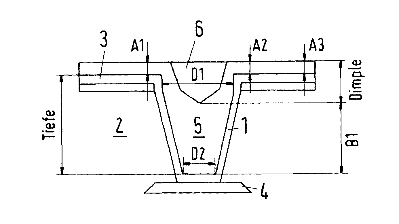
[0077]The printed circuit boards were coated with copper with different leveler content in the bath. First of all a test was carried out without leveler for comparison purposes. Then tests according to the invention were carried out with increasing leveler content. The evaluation was effected by removing micro-sections at a previously defined position on the printed circuit board. The dimple was used as a measurement for the filling of a BMV. FIG. 2 shows the determining of this test parameter in a schematic manner: The wall of a BMV made electrically conductive by means of conventional methods is given the numeral 1. This conductive layer merges on the surface of the adjoining photoresist layer 2 into a plated surface 3, for example a conductor path. The base of the plating in the BMV is in electrical contact with a copper layer 4. The BMV is filled with copper 5 using the method according to the invention. However, a top region 6 is no...

example 2

OF THE INVENTION

[0083]NH2-Gly-Leu-OH exhibits BMV filling characteristics. In contrast to conventional levelers, however, the amino acids and peptides never cause a ski slope. This advantageous effect can be used to selectively influence the line shape in the baths for the filling of BMVs without impairing the BMV filling. To investigate the line shape a test board was coppered, said board having channels as produced by photoresists. The said channels were filled with copper under the specified conditions, NH2-Gly-Leu-OH, as specified in Example 1 of the Invention, being used as the leveler. The copper layer grew uniformly and formed a rectangular structure 2 in the trench (FIG. 6).

[0084]This is not observed, however, with conventional levelers that are usually used for filling vias. For a comparative test of this type, NH2-Gly-Leu-OH was not used as leveler but rather an Atotech Cupracid® HL bath with BMV filling characteristics. In this case, a concave deposition shape was observe...


PUM

PropertyMeasurementUnit
mean molecular weightaaaaaaaaaa
concentrationaaaaaaaaaa

Abstract

An aqueous, acid bath for the electrolytic deposition of copper contains at least one copper ion source, at least one acid ion source, at least one brightener compound, and at least one leveler compound, and generates a very uniform copper deposit in particular in blind micro vias (BMVs) and trenches. The leveler compound is selected from among synthetically produced non-functionalized peptides, synthetically produced functionalized peptides, and synthetically produced functionalized amino acids.

Description

FIELD OF THE INVENTION[0001]The invention relates to an aqueous, acid bath and to a method for the electrolytic deposition of copper, in particular for filling blind micro vias (BMVs), through vias, trenches and similar structures on printed circuit boards, chip carriers and semiconductor wafers.BACKGROUND OF THE INVENTION[0002]Adding numerous different organic additives to acid electrolytic copper baths is known in order to enable the decorative and functional characteristics of the copper coatings to be controlled. Above all, brighteners and carriers are added to the baths in order to obtain bright deposits. In addition, organic compounds are used as additives to the coppering baths during the production of printed circuit boards, chip carriers and semiconductor wafers, and these compounds are to act as levelers and enable as uniform a deposition of copper as possible in and on different regions of the surface of the printed circuit board or of the structure of the printed circuit...

Claims


Application Information

Patent Timeline
Patent Type & Authority Patents(United States)
IPC IPC(8): C25D3/38C25D5/02
CPCH05K3/421H05K3/423C25D5/18C25D3/38C25D5/611C25D1/02
Inventor BRUNNER, HEIKOROELFS, BERNDROHDE, DIRKPLIET, THOMAS
Owner ATOTECH DEUT GMBH
Why Eureka
Try Eureka