Organic electroluminescence display device and manufacturing method thereof

a technology of electroluminescence display and organic electroluminescence, which is applied in the direction of discharge tube luminescnet screen, organic semiconductor device, discharge tube/lamp details, etc., can solve the problems of inability to achieve sufficient performance, inability to meet the requirements of use, etc. , to achieve the effect of improving the barrier property against moisture, low hydrogen content and high density

Active Publication Date: 2014-03-25
SAMSUNG DISPLAY CO LTD
View PDF31 Cites 3 Cited by
  • Summary
  • Abstract
  • Description
  • Claims
  • Application Information

AI Technical Summary

Benefits of technology

[0014]Moreover, because the film formation is performed at low temperature, foreign substances resulting from unreacted products are also likely to be generated. Besides, the temperature in the film formation process is likely to vary, and hence film quality significantly varies. The idea of increasing film thickness may be considered, but this idea is not realistic because the film formation rate is low, and in addition, the amount of equipment investment is increased.
[0015]Therefore, it is an object of the present invention to improve life property of an organic EL display device by obtaining a protective film having a high film formation rate and an excellent waterproof effect.
[0052]According to the present invention, as the protective film for the organic EL display device, it is possible to obtain the SiNxOy film which may be formed by low temperature film formation, and in which foreign substances resulting from unreacted products are few, and the hydrogen content is low and the density is high as compared with a film formed by a CVD method. Accordingly, it is possible to improve a barrier property against moisture, and to realize a long lifetime of the organic EL display device. Further, with the combined use of magnesium oxide, the protective film is allowed to have a higher moisture-proof effect.
[0053]Since a reactive plasma deposition (RPD) method and a sputtering method may be applied, the use of an evaporation mask for a panel terminal section is enabled. Further, since the need for semiconductor gas introduction equipment and waste gas processing equipment is eliminated, the equipment cost may be reduced. Accordingly, the cost of forming the protective film in the organic EL display device may be reduced.

Problems solved by technology

However, in the case of an SiN film that is normally used as a semiconductor protective film formed by a CVD method, if film formation is performed at a temperature as low as 100° C. or less (80° C. or less if possible) which is required for formation of a protective film for an organic EL display device, sufficient performance cannot necessarily be obtained because the hydrogen content is high and the density is low due to appearance of Si—H and N—H.
Moreover, because the film formation is performed at low temperature, foreign substances resulting from unreacted products are also likely to be generated.
The idea of increasing film thickness may be considered, but this idea is not realistic because the film formation rate is low, and in addition, the amount of equipment investment is increased.

Method used


Image

  • Organic electroluminescence display device and manufacturing method thereof
  • Organic electroluminescence display device and manufacturing method thereof
  • Organic electroluminescence display device and manufacturing method thereof

Examples


embodiment 1

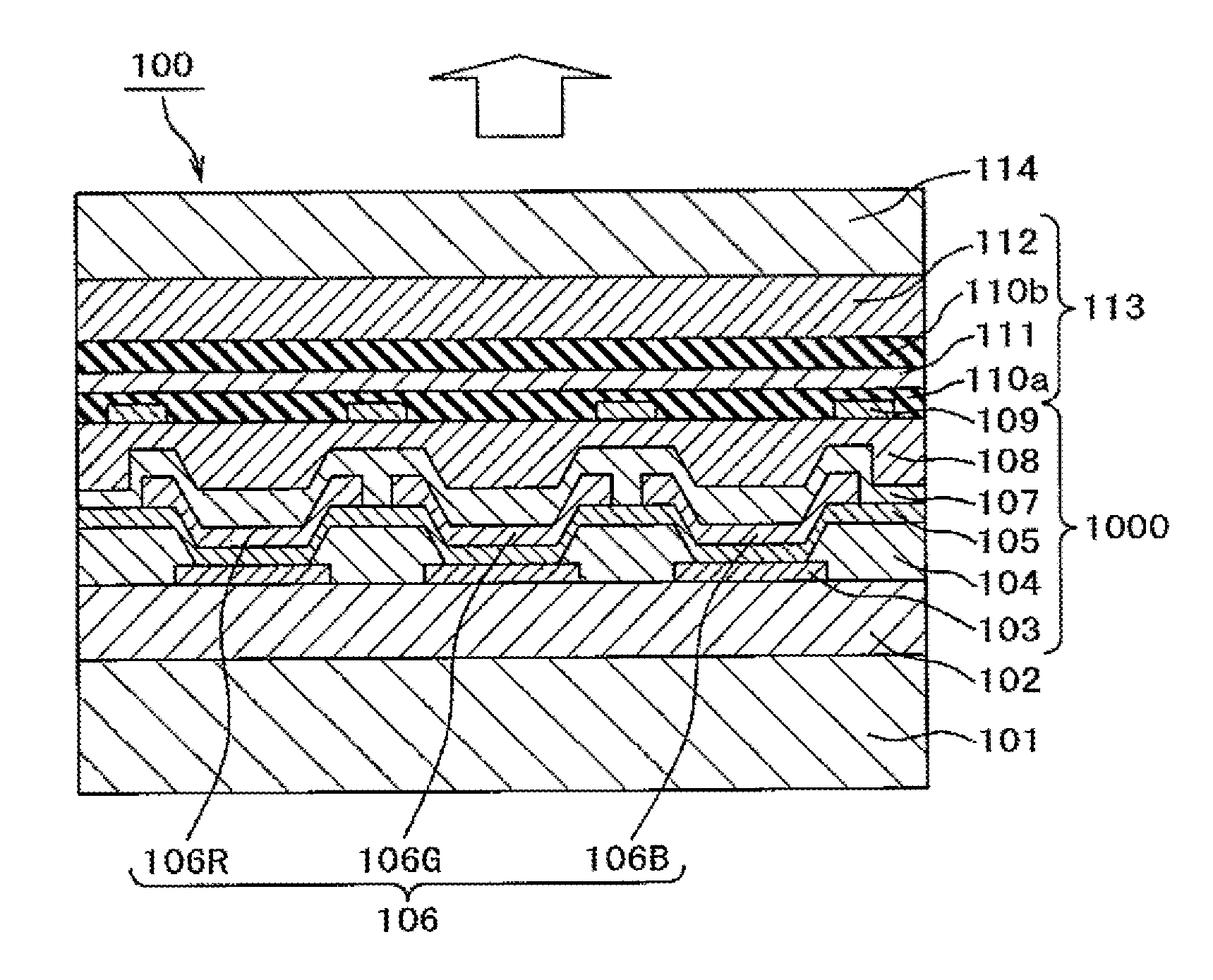
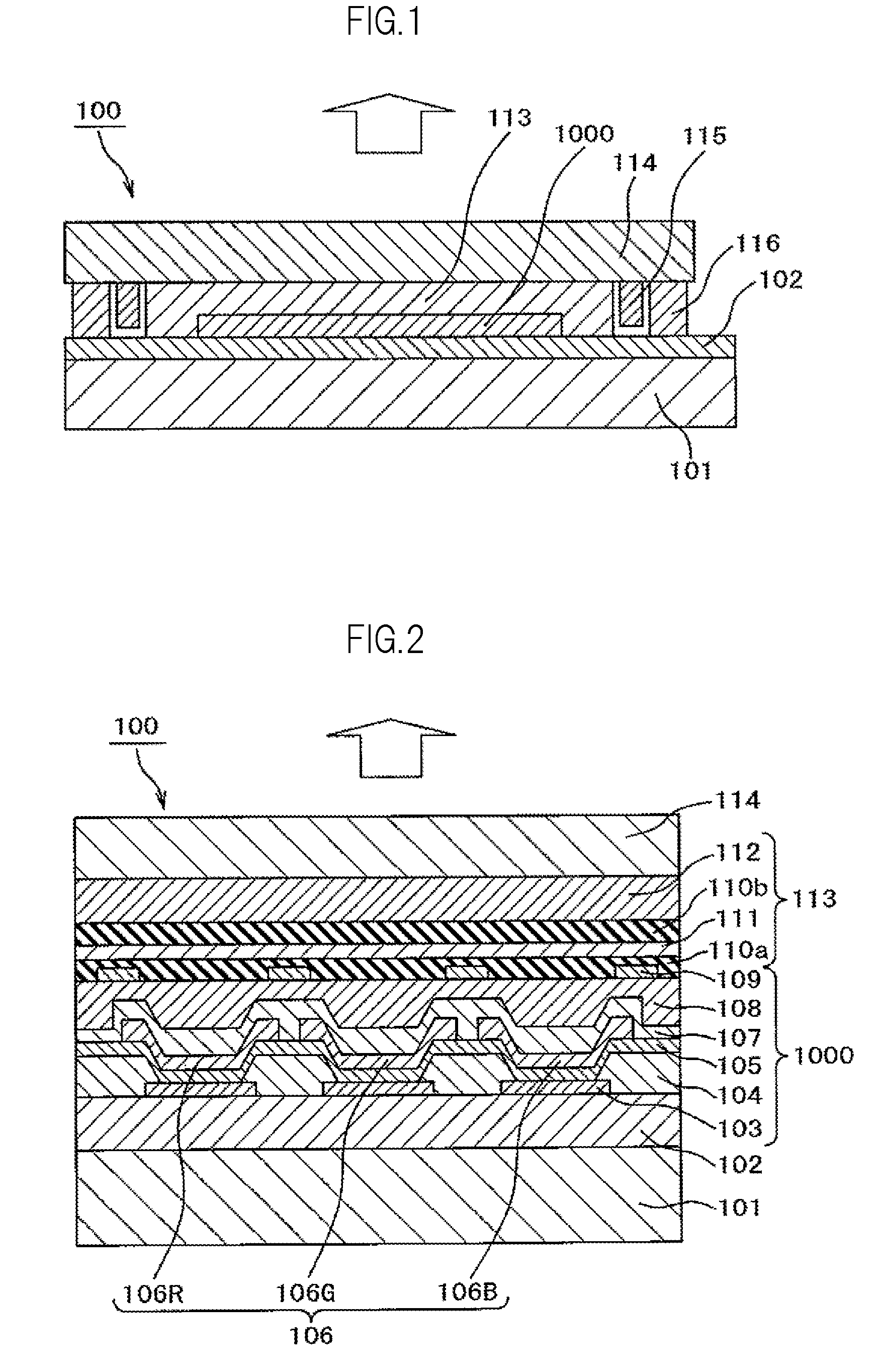
[0073]FIG. 1 is a cross-sectional view illustrating a main portion of an organic EL panel 100. In FIG. 1, the organic EL panel 100 includes: a circuit board 101 including a glass substrate; a circuit formation section 102 such as a thin film transistor (TFT); an organic EL element section 1000 having an organic EL element formed thereon; a protective film 113 formed so as to cover the organic EL element section 1000; a sealing glass 114; a drying agent 115; and a sealing agent 116. The outline arrow indicates a direction of light emission, and in a case of this embodiment, light is to be taken out from the sealing glass 114 side.

[0074]The organic EL element section 1000 is sealed with the sealing glass 114, the protective film 113, the sealing agent 116, and the circuit board 101 including the circuit formation section 102. An organic film made of acrylic, polyimide or the like, or an inorganic insulating film such as an Si oxide film or an Si nitride film is formed as a planarizing...

embodiment 2

[0107]This embodiment provides an example of application of the present invention to a bottom emission type organic EL panel, and is similar to Embodiment 1 except for this point. FIG. 7 is a cross-sectional view illustrating a main portion of an organic EL panel 100. In FIG. 7, the organic EL panel 100 includes: a circuit board 101 such as a glass substrate; a circuit formation section 102 including a thin film transistor (TFT); an organic EL element section 1000 having an organic EL element formed thereon; a protective film 113 formed so as to cover the organic EL element section 1000; a sealing glass 114; a drying agent 115; and a sealing agent 116. The outline arrow indicates a direction of light emission, and in a case of this embodiment, light is to be taken out from the circuit board 101 side. The organic EL element section 1000 is sealed with the sealing glass 114, the protective film 113, the sealing agent 116, and the circuit board 101 including the circuit formation secti...

embodiment 3

[0112]This embodiment provides an example of application of the present invention to an organic EL panel in which hollow sealing is provided, and is similar to Embodiment 1 except for this point. FIG. 9 is a cross-sectional view illustrating a main portion of an organic EL panel 100. In FIG. 9, the organic EL panel 100 includes a circuit board 101 such as a glass substrate; a circuit formation section 102 including a thin film transistor (TFT); an organic EL element section 1000 having an organic EL element formed thereon; a protective film 113 formed so as to cover the organic EL element section 1000; a sealing glass 114; a drying agent 115; and a sealing agent 116.

[0113]In a case of this embodiment, a sealing space 117 is newly formed between the sealing glass 114 and the protective film 113. This embodiment differs in this point from Embodiment 1, and is similar in other points to Embodiment 1. The outlinear row indicates a direction of light emission, and in the case of this emb...


PUM

PropertyMeasurementUnit
temperatureaaaaaaaaaa

Abstract

An organic EL element section (1000) is formed on a circuit formation section (102) formed on a circuit board (101). The organic EL element section (1000) is covered with a protective layer (113) including an SiNxOy film. The SiNxOy film has infrared absorption characteristics including: an Si—O—Si stretching vibration absorption peak appearing at energy lower than 1,000 cm−1; an absorption intensity of an Si—N stretching vibration absorption peak appearing in the vicinity of around 870 cm−1 which is 0.75 or more times an absorption intensity of the Si—O—Si stretching vibration absorption peak; and an absorption peak intensity in a range of 2,000 to 4,000 cm−1, which is 5% or less of the absorption intensity of the Si—N stretching vibration absorption peak. Thus, the protective film having an excellent moisture-blocking property may be obtained, and life property of an organic EL display device may be improved.

Description

CROSS-REFERENCE TO RELATED APPLICATION[0001]The present application claims priority from Japanese application JP2007-288956 filed on Nov. 6, 2007, the content of which is hereby incorporated by reference into this application.BACKGROUND OF THE INVENTION[0002]1. Field of the Invention[0003]The present invention relates to an organic electroluminescence (EL) display device, in particular, a reliable top emission type organic EL display device in which generation of a dark spot caused by moisture is suppressed, and a method of manufacturing the same.[0004]2. Description of the Related Art[0005]In an organic EL display device, an organic EL layer is sandwiched between a lower electrode (first electrode) and an upper electrode (second electrode), a constant voltage is applied to the upper electrode, and a data signal voltage is applied to the lower electrode so as to control light emission of the organic EL layer, thereby forming an image. Supply of data signal voltage to the lower elect...

Claims


Application Information

Patent Timeline
Patent Type & Authority Patents(United States)
IPC IPC(8): H01L51/50H01L51/56C23C16/00H01L51/52
CPCH01L51/5237H01L2251/5315H10K50/8445H10K50/841H10K2102/3026H05B33/04H05B33/22H10K71/00H10K50/85H10K50/844H10K50/84
Inventor MATSUZAKI, EIJIISHII, YOSHINORIKASE, SATORU
Owner SAMSUNG DISPLAY CO LTD
Why Eureka
Try Eureka