Display device and method for production thereof

a technology of a display device and a production method, which is applied in the direction of discharge tube/lamp details, organic semiconductor devices, discharge tubes/lights, etc., can solve the problems of increasing the power consumption of the device, large voltage drop across the oxidized part, and the auxiliary wiring made from the same material as the electrode is subject to surface oxidation, etc., to achieve the effect of improving yield and reducing contact resistan

Active Publication Date: 2014-04-08
SONY CORP
View PDF12 Cites 2 Cited by
  • Summary
  • Abstract
  • Description
  • Claims
  • Application Information

AI Technical Summary

Benefits of technology

[0011]However, the technology disclosed in Patent Document 1 mentioned above has the disadvantage that the auxiliary wiring made from the same material as the electrode is subject to surface oxidation if the electrode on the driving panel is made of aluminum or aluminum alloy. Surface oxidation results in an increased connecting resistance between the auxiliary wiring and the electrode through which light emerges and hence results in a large voltage drop across the oxidized part. This voltage drop in turn increases the power consumption of the device.
[0013]The present embodiment was completed in view of the forgoing. It is desirable to provide a display device of top emitting type and a method for production thereof, the display device achieving low power consumption without resorting to auxiliary wiring and also having an improved display quality.
[0018]The display device and the method for production thereof according to the present embodiment offer the following advantages. The second electrode and the auxiliary wiring are electrically connected to each other through the conductive contact part; therefore, even though the auxiliary wiring suffers surface oxidation, the contact resistance does not increase. Thus the display device ensures low power consumption and improved display device regardless of the structure of the auxiliary wiring.
[0020]The wiring layer close to the driving elements is placed in the lower layer of the contact part, so that steps due to the planarized layer become smaller and the contact resistance decreases. Thus it is possible to improve yields without resorting to increasing the contact resistance.

Problems solved by technology

However, the technology disclosed in Patent Document 1 mentioned above has the disadvantage that the auxiliary wiring made from the same material as the electrode is subject to surface oxidation if the electrode on the driving panel is made of aluminum or aluminum alloy.
Surface oxidation results in an increased connecting resistance between the auxiliary wiring and the electrode through which light emerges and hence results in a large voltage drop across the oxidized part.
This voltage drop in turn increases the power consumption of the device.
As mentioned above, the existing technology involves difficulties in avoiding increased power consumption without resorting to the auxiliary wiring and difficulties in improving the display quality by realizing even voltage distribution throughout the electrode through which light emerges.

Method used


Image

  • Display device and method for production thereof
  • Display device and method for production thereof
  • Display device and method for production thereof

Examples


first embodiment

The First Embodiment

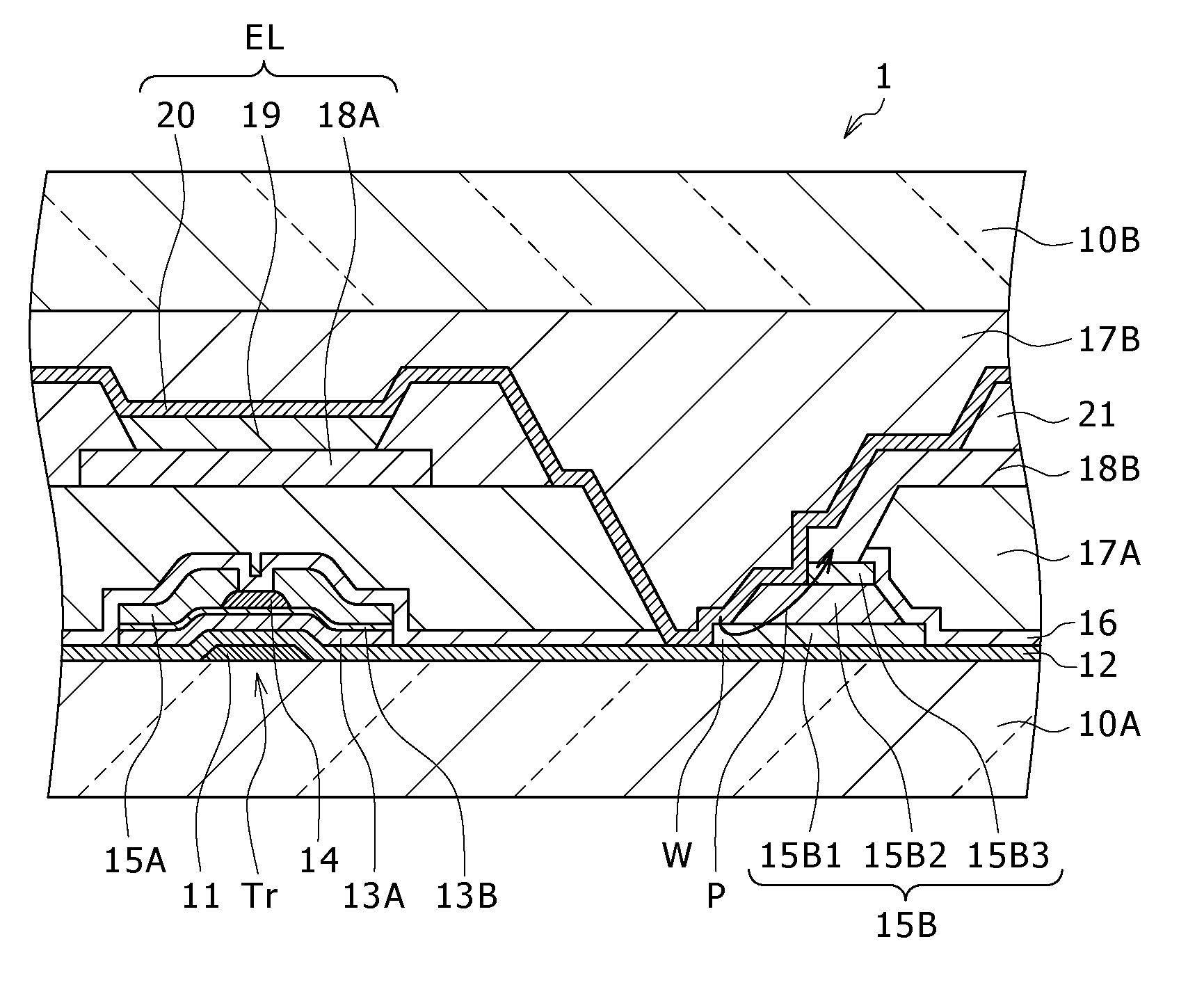
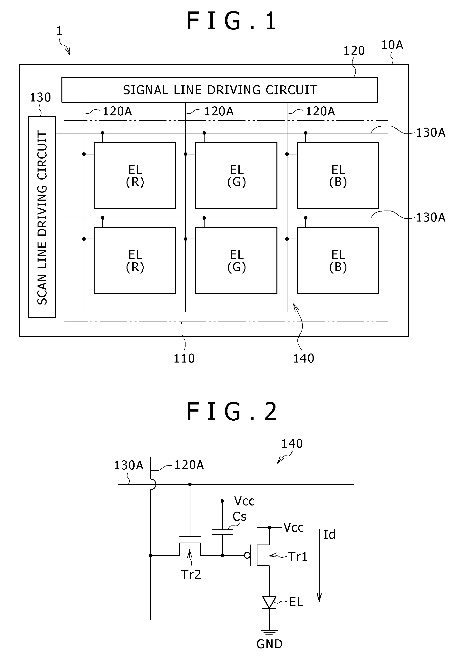
[0049]FIG. 1 is a diagram showing the structure of the display device (organic EL display device) pertaining to the first embodiment of the present invention. The organic EL display device 1 is one which is used as an organic color display device of very thin type. It is composed of a transparent substrate 10A and a plurality of organic EL elements (EL) arranged thereon in a matrix pattern so as to form the display region 110. It also has a signal driving circuit 120 and a scan line driving circuit 130 (both for image display), which are formed along the sides of the display region 110.

[0050]The display region 110 has the pixel driving circuit 140 formed therein. FIG. 2 is a diagram showing an example of the pixel driving circuit 140. The pixel driving circuit 140 is a driving circuit of active type, which is formed under the first electrode 18A (mentioned later) and is composed of a driving transistor Tr1, a writing transistor Tr2, a capacitor Cs (placed between...

second embodiment

The Second Embodiment

[0098]The following deals with the display device pertaining to the second embodiment of the present invention. The constituents common to the first and second embodiments are given the same symbols and their explanation is not repeated.

[0099]FIG. 11 is a sectional view showing the structure of the contact part 25B of the display device (organic EL display device) pertaining to this embodiment. The contact part 25B has on the transparent substrate 11A the low-resistance wiring layer 26 as the lowermost layer which is identical with the source signal line or gate wiring connected to the thin film transistor Tr. The low-resistance wiring layer 26 is 500 nm thick and has the layer identical with the gate electrode 11, the gate insulating layer 12, the silicon film 13A, the stopper insulating film 14, and the n+-amorphous silicon film 13B which are sequentially formed thereon upward. The low-resistance wiring layer 26 prevents the gate wiring, the source signal line...

third embodiment

The Third Embodiment

[0108]FIG. 14 is a diagram showing the plane structure of the display region 110 of the organic EL display device 1 according to the third embodiment of the present invention. FIG. 15 is a sectional view taken along the line XV-XV in FIG. 14. This organic EL display device 1 is identical in structure with the one according to the first embodiment mentioned above, except that the auxiliary wiring 15C has the same layered structure as the contact part 15B and is formed integrally with the contact part 15B. Thus, the corresponding constituents are given the same reference characters.

[0109]This embodiment is identical with the first embodiment in that the same structure is adopted for the transparent substrates 10A and 10B, the thin film transistor Tr, the wiring layer 15A, the contact part 15B, the protective insulating film 16, the planarized insulating film 17A, the electrode insulating film 21, the sealing resin 17B, and the organic EL element (EL).

[0110]The auxi...


PUM


Abstract

A display device having a plurality of driving elements and wiring parts electrically connected to the driving parts, the display device includes: a plurality of first electrodes which are formed in correspondence to each driving element on the driving elements and the wiring parts; a plurality of light-emitting parts which are each formed on the first electrodes; a common second electrode which is formed from a material that transmits light from the light-emitting part and is formed on the light-emitting parts; auxiliary wiring parts with a lower resistance than the second electrodes; and contact parts which are formed in laminate structure from a plurality of conductive layers and which electrically connect the second electrodes and the auxiliary wirings with each other, with at least the lowermost conductive layer of the conductive layers of the contact parts being in direct contact with the second electrode.

Description

CROSS REFERENCES TO RELATED APPLICATIONS[0001]The present invention contains subject matter related to Japanese Patent Application JP 2008-123004, and JP 2007-326595, both filed in the Japan Patent Office on May 9, 2008, and on Dec. 18, 2007, respectively, the entire contents of which being incorporated herein by reference.BACKGROUND OF THE INVENTION[0002]1. Field of the Invention[0003]The present invention relates to a display device of top emitting type and a method for production thereof.[0004]2. Description of the Related Art[0005]Among recent flat panel display devices attracting attention is the organic EL display device which displays images by means of organic EL (Electro Luminescence). The organic EL display device is a wide viewing angle and a low electric power consumption, the former being due to the fact that it utilizes emission from organic EL elements themselves. In addition, being highly responsive to high-definition high-speed video signals, the organic EL display ...

Claims


Application Information

Patent Timeline
Patent Type & Authority Patents(United States)
IPC IPC(8): H05B33/26
CPCH01L27/3276H01L51/5234H01L51/5206H01L51/5228H01L2251/5315H01L27/1214H01L27/124H10K59/1315H10K59/131H10K50/814H10K50/824H10K50/828H10K2102/3026
Inventor HAYASHI, NAOKIHIROMASU, YASUNOBUFUJIOKA, HIROFUMI
Owner SONY CORP
Why Eureka
Try Eureka