CMOS integrated micromechanical resonators and methods for fabricating the same

a micromechanical resonator and integrated technology, applied in the direction of microstructural devices, acceleration measurement using interia forces, instruments, etc., can solve the problems of significant retooling and/or modification of the cmos foundry, the need for two foundry sequences to complete the device fabrication, and the standard cmos foundry process must include non-standard mems process sequences, etc., to achieve improved actuation and detection capabilities, improved yield, and reduced power consumption

Inactive Publication Date: 2014-04-22
THE UNITED STATES OF AMERICA AS REPRESENTED BY THE SECRETARY OF THE NAVY +1
View PDF14 Cites 1 Cited by
  • Summary
  • Abstract
  • Description
  • Claims
  • Application Information

AI Technical Summary

Benefits of technology

[0017]The present invention addresses the needs described above by providing an improved method for integrating MEMS / NEMS devices and CMOS circuits using a standard CMOS foundry process. An improved process is needed such that the MEMS devices are characterized by improved actuation and detection capabilities, lower power consumption, and a greater yield, without the need for post fabrication stiction-inhibiting processes.

Problems solved by technology

Essentially, the drawback associated with each of these approaches is that they require two foundry sequences to complete the device fabrication.
One drawback to this approach is that the standard CMOS foundry process must be modified to include non-standard MEMS process sequences.
This may require a significant re-tooling and / or modification of the CMOS foundry and directly translates to higher costs.
The costs may be prohibitive because a given CMOS foundry may be unwilling to make the modifications in light of their obligations to their customer base.
The disruptions to the foundry's work flow may not be worth the trouble.
In the methods described above, the integration of MEMS / NEMS devices and CMOS circuits has not been effectively realized because of incompatibilities with MEMS / NEMS processes and standardized CMOS foundry processes.
However, the bridge and cantilever structures that may be fabricated by the contemplated method are very small.
The drawbacks associated with this proposed method are that the capacitor pick-up surfaces are disposed “in-plane.” Another drawback relates to the fact that the surface area for capacitive pick-up is on the order of about 1 μm2.
As the linewidth becomes smaller, more sophisticated (and hence, more expensive) illumination assemblies are required.
Another drawback of the standard CMOS process under consideration relates to the fabrication of a MEMS device and its subsequent release.
Unfortunately, when the etchant evaporates, it has a tendency to introduce a suction force such that the bridge is forced downwardly and sticks to the underlying substrate.
Accordingly, MEMS devices that may be fabricated using this technique would have a very low yield rate.
As noted above, stiction is often an issue in standard MEMS devices (i.e., those devices fabricated using standard non-CMOS techniques).
First, it is relatively expensive.
Second, it introduces additional non-CMOS steps into the back end of the process.
Accordingly, it defeats the very purpose of using a standard CMOS foundry process to produce MEMS devices; i.e., to avoid expensive post fabrication processing.

Method used


Image

  • CMOS integrated micromechanical resonators and methods for fabricating the same
  • CMOS integrated micromechanical resonators and methods for fabricating the same
  • CMOS integrated micromechanical resonators and methods for fabricating the same

Examples


Embodiment Construction

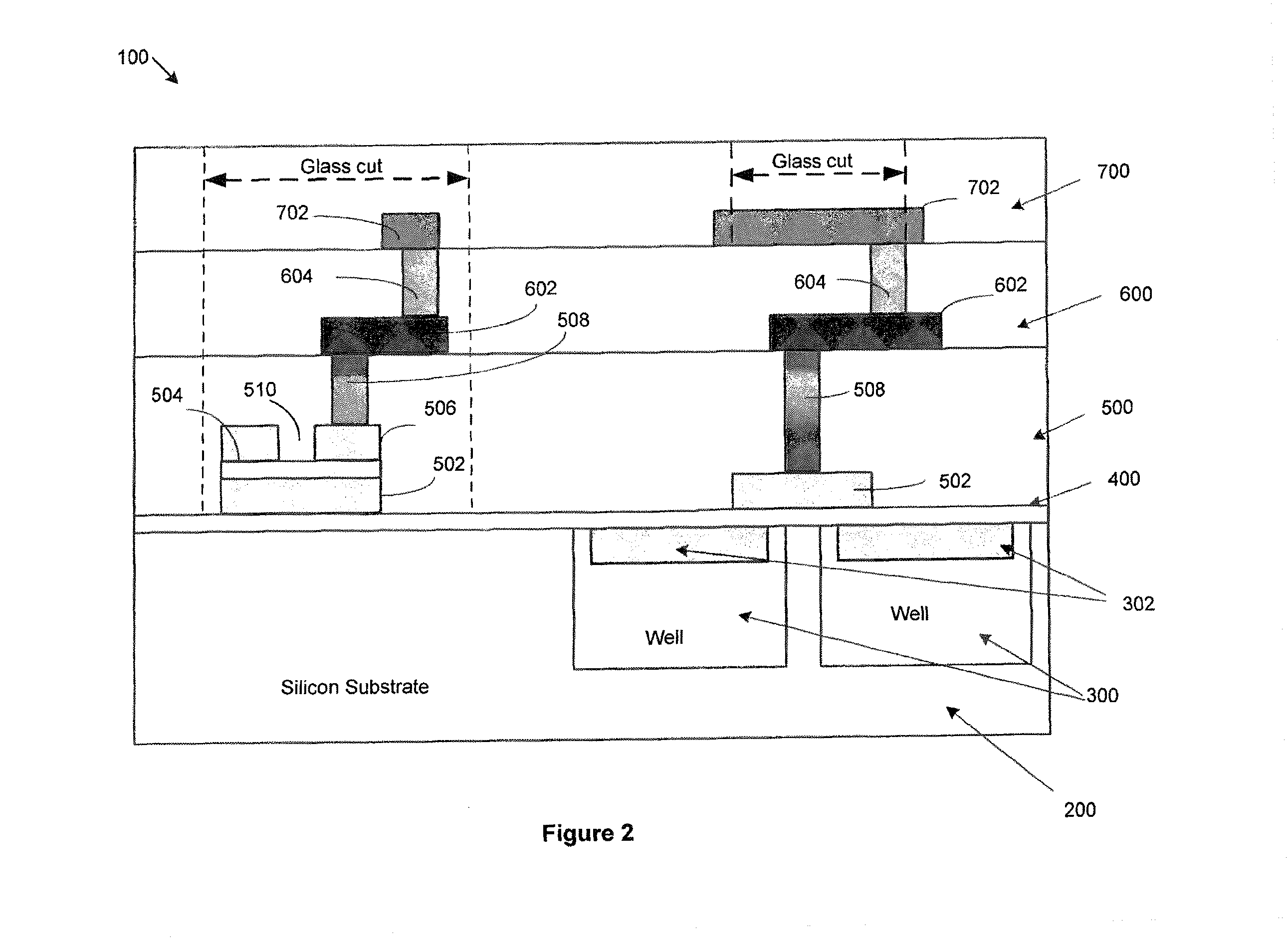
[0032]Reference will now be made in detail to the present exemplary embodiments of the invention, examples of which are illustrated in the accompanying drawings. Wherever possible, the same reference numbers will be used throughout the drawings to refer to the same or like parts. An exemplary embodiment of the resonator device of the present invention is shown in FIG. 5, and is designated generally throughout by reference numeral 10.

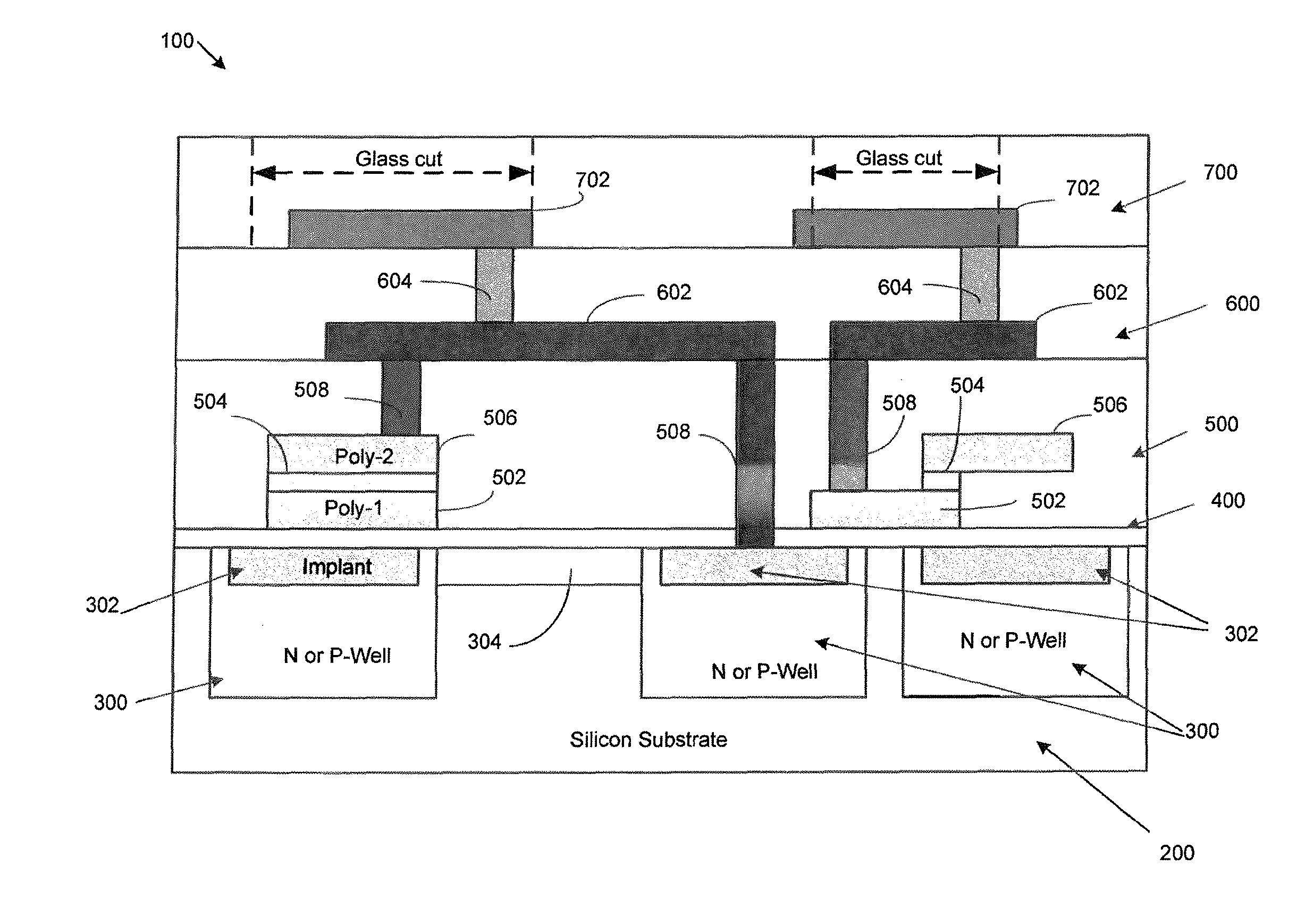
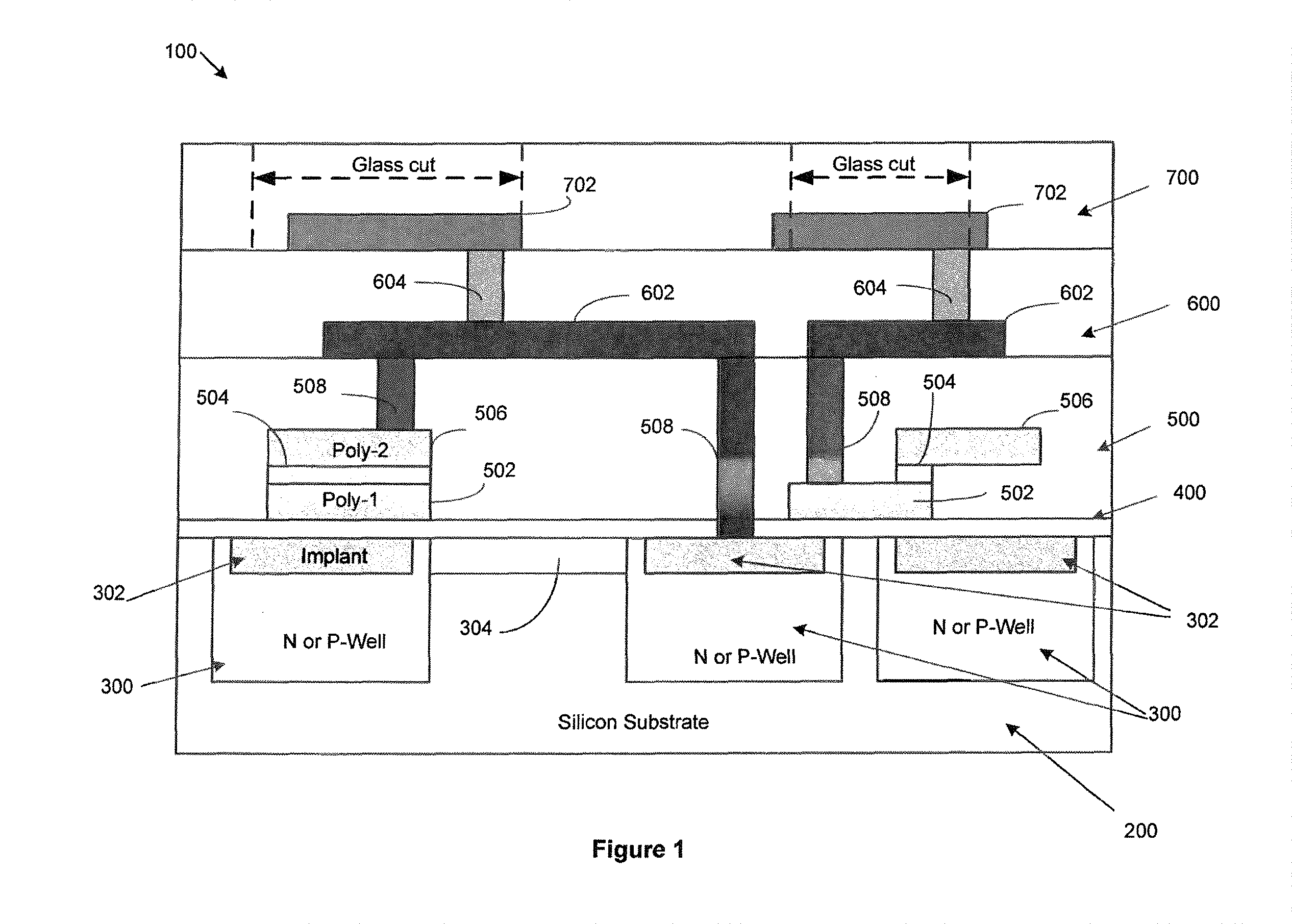
[0033]As embodied herein, and depicted in FIG. 1, a cross-sectional schematic of the standard film stack for the AMIS ABN 1.5 μm fabrication process is depicted. The film stack shown in FIG. 1 corresponds, of course, to a standard layer map much like the one depicted in Table 1 above. The AMIS ABN 1.5 μm film stack is a two metal layer, two polysilicon layer film stack.

[0034]Proceeding from bottom to top, layer 200 corresponds to a silicon substrate. Once the silicon substrate 200 is provided, wells 300 are formed therein. The wells are formed by applyin...


PUM

PropertyMeasurementUnit
distanceaaaaaaaaaa
distanceaaaaaaaaaa
diameteraaaaaaaaaa

Abstract

The present invention is directed to a CMOS integrated micromechanical device fabricated in accordance with a standard CMOS foundry fabrication process. The standard CMOS foundry fabrication process is characterized by a predetermined layer map and a predetermined set of fabrication rules. The device includes a semiconductor substrate formed or provided in accordance with the predetermined layer map and the predetermined set of fabrication rules. A MEMS resonator device is fabricated in accordance with the predetermined layer map and the predetermined set of fabrication rules. The MEMS resonator device includes a micromechanical resonator structure having a surface area greater than or equal to approximately 20 square microns. At least one CMOS circuit is coupled to the MEMS resonator member. The at least one CMOS circuit is also fabricated in accordance with the predetermined layer map and the predetermined set of fabrication rules.

Description

CROSS-REFERENCE TO RELATED APPLICATIONS[0001]This is application claims the benefit of priority under 35 U.S.C. §119(e) to U.S. Provisional Patent Application Ser. No. 61 / 075,855 filed on Jun. 26, 2008 and U.S. Provisional Patent Application Ser. No. 61 / 075,773 filed on Jun. 26, 2008, the contents of which is relied upon and incorporated herein by reference in their entirety.GOVERNMENT SPONSORSHIP[0002]This invention was made with Government support under: Contract No. N0001408WX30004 awarded by the Office of Naval Research (ONR); and Grant No. HR0011-06-1-0042 awarded by the Department of Defense, specifically DARPA. The Government has certain rights in the invention.BACKGROUND OF THE INVENTION[0003]1. Field of the Invention[0004]The present invention relates generally to fabricating micromechanical semiconductor devices, and particularly to MEMS / NEMS devices using standard CMOS fabrication processes.[0005]2. Technical Background[0006]The performance of radio frequency (RF), wirele...

Claims


Application Information

Patent Timeline
Patent Type & Authority Patents(United States)
IPC IPC(8): H01L29/82
CPCB81C1/00246B81B2201/0271Y10T29/49007
Inventor PARPIA, JEEVAK M.CRAIGHEAD, HAROLD G.CROSS, JOSHUA D.ILIC, BOJAN ROBERTZALALUTDINOV, MAXIM K.BALDWIN, JEFFREY W.HOUSTON, BRIAN H.
Owner THE UNITED STATES OF AMERICA AS REPRESENTED BY THE SECRETARY OF THE NAVY
Why Eureka
Try Eureka