
Organic electroluminescence device, method of manufacturing organic electroluminescence device, display apparatus and illumination apparatus

a technology of organic electroluminescence and electroluminescence device, which is applied in the manufacture of electrode systems, electric discharge tubes/lamps, and discharge tubes luminescent screens, etc., can solve the problems of exacerbating el properties, deterioration of organic electroluminescence device luminous efficiency and durability, and insufficient luminous efficiency, durability and color reproducibility, etc., to achieve high luminous efficiency, reduce manufacturing cost, and reduce the effect of drive voltag

Active Publication Date: 2014-05-13
UDC IRELAND
View PDF8 Cites 0 Cited by
  • Summary
  • Abstract
  • Description
  • Claims
  • Application Information

AI Technical Summary

Benefits of technology

The invention aims to create an organic electroluminescence device that is highly efficient, durable, and can produce vivid colors. Additionally, it seeks to reduce the required drive voltage and lower manufacturing costs. The patent text presents a method to achieve this goal.

Problems solved by technology

The coating-type organic EL devices disclosed in U.S. Pat. No. 7,453,200 and JP Patent 3541294, however, have problems that, because each of their light emitting layers is formed of a single layer, they are insufficient in luminous efficiency, durability and color reproducibility when two or more kinds of light emitting materials are incorporated into each of their light emitting layers for the purpose of obtaining a desired color of light emission (e.g. white-light emission in view of the use in illumination apparatus).
However, the coating in accordance with a spin coating method tends to cause damage to the underlying layer, and hence the organic EL device occasionally underwent deterioration in luminous efficiency and durability.
According to such a method, however, the residue structure of the polymerization catalyst is left in each light emitting layer, which caused a problem of exacerbating EL properties, especially durability of the device.

Method used


Image

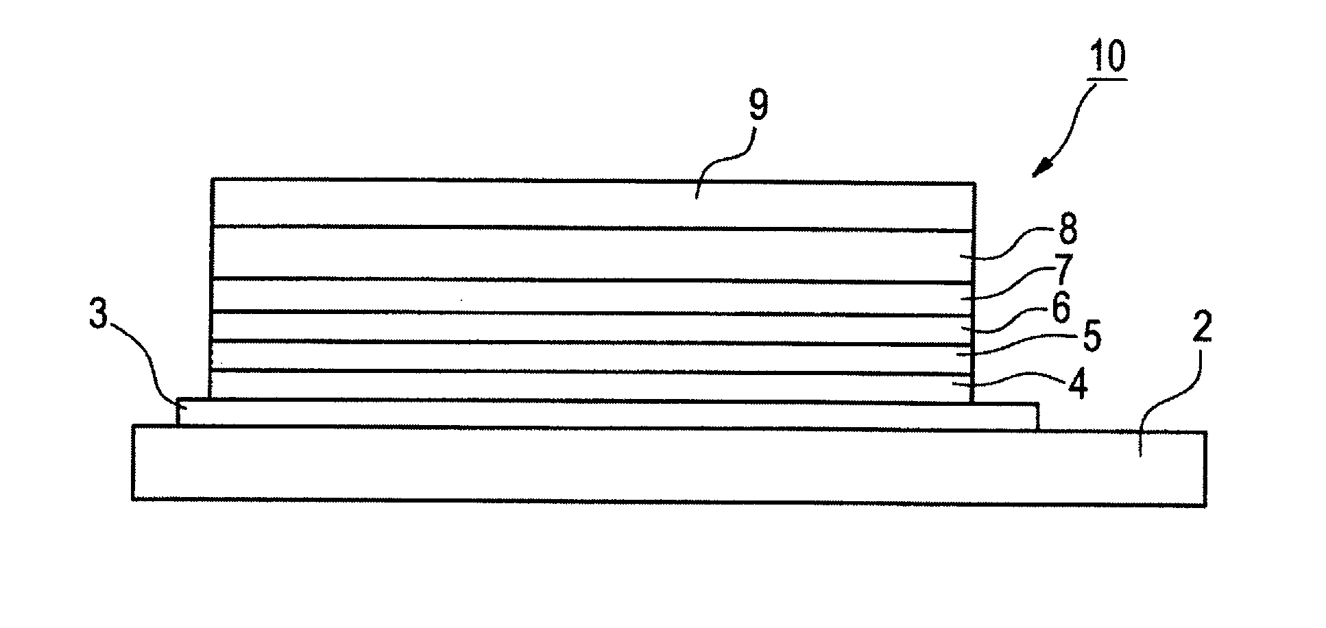
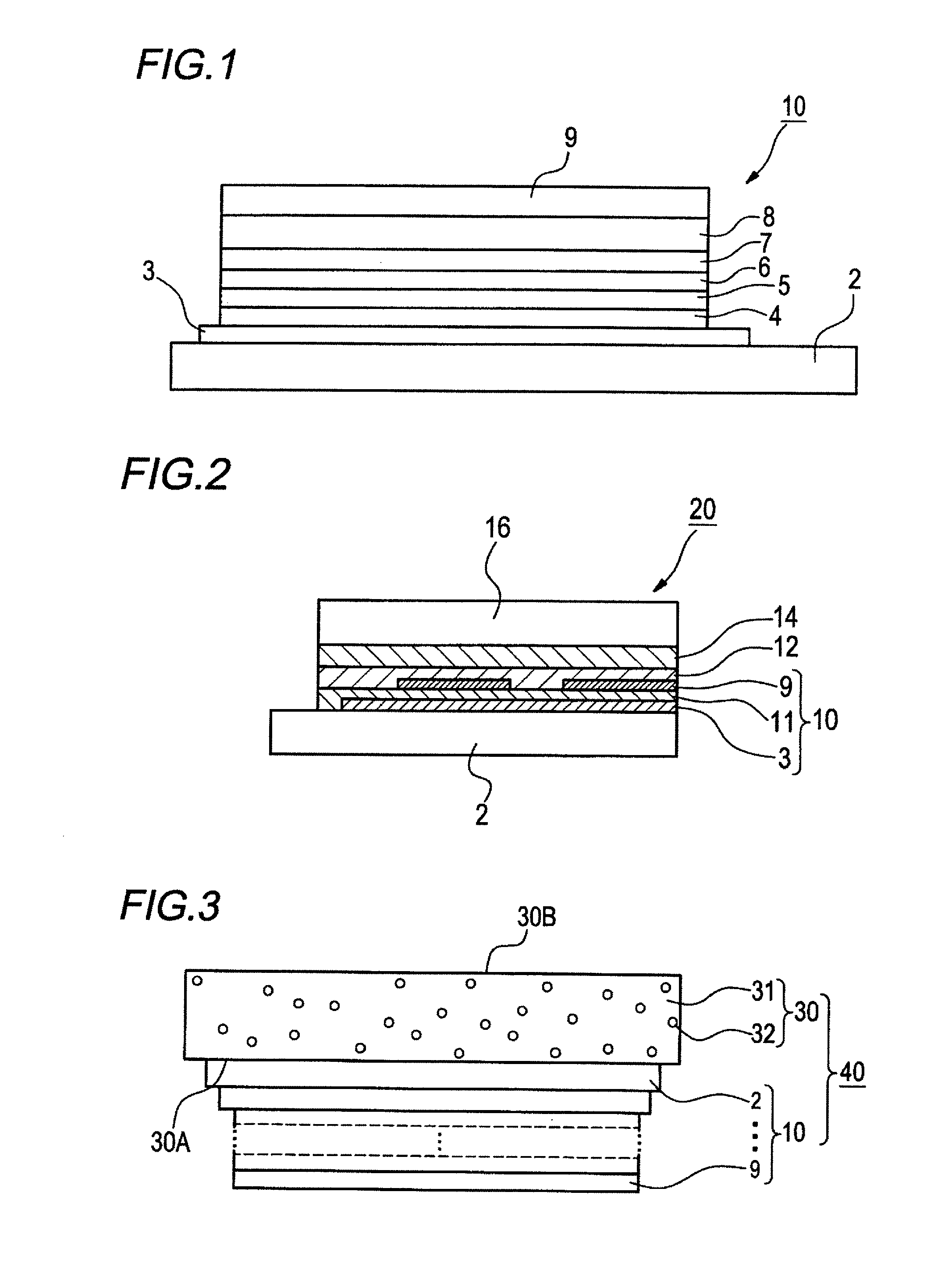
  • Organic electroluminescence device, method of manufacturing organic electroluminescence device, display apparatus and illumination apparatus
  • Organic electroluminescence device, method of manufacturing organic electroluminescence device, display apparatus and illumination apparatus
  • Organic electroluminescence device, method of manufacturing organic electroluminescence device, display apparatus and illumination apparatus

Examples


example 1

[0191]A glass substrate having a deposition layer of iridium tin oxide (abbreviated as ITO) (manufactured by GEOMATEC Corporation, surface resistance: 10 Ω / sq., size: 0.5 mm thickness, 2.5 by 2.5 centimeters square) was placed in a cleaning vessel, and subjected to ultrasonic cleaning in 2-propanol. Then, UV-ozone treatment was given to the cleaned substrate for 30 minutes. On the thus obtained transparent anode, the following layers were provided in succession by use of a spraying method. In the formation of each layer, the carrier gas (N2) quantity of an aerosol used and the size of liquid particles in the aerosol were adjusted to 1 L / min and 1 μm, respectively.

[0192](1) Hole transporting layer (40 nm): By using the spraying method, poly(3,4-ethylenedioxythiophene)poly(styrenesulfonate) (PEDOT:PSS) (1 mass % aqueous dispersion liquid, AI4083, manufactured by Bayer AG, mass-average molecular weight: 10,000) was coated on the transparent anode in an amount to give a thickness of 40 ...

example 2

[0195]By carrying out the same procedure as in Example 1, except that the first light emitting layer was formed in the following step, an organic EL device of Example 2 was made wherein each of the hole transporting layer, the second light emitting layer and the third light emitting layer was formed in film according to the spraying method and the first light emitting layer was formed in film according to a deposition method.

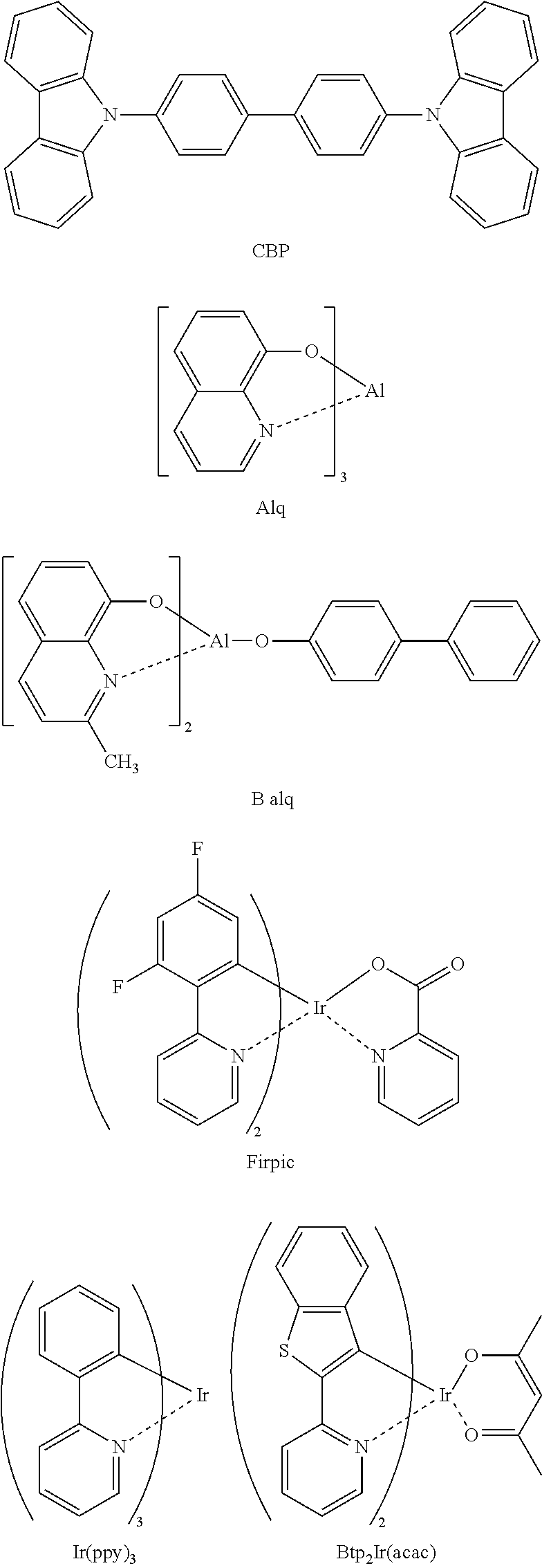
[0196](2) First light emitting layer (Blue light emitting layer) (10 nm): By using a vacuum deposition method, CBP and Firpic were deposited on the hole transporting layer in amounts to have a ratio of 85:15 by mass and give a thickness of 10 nm to a first light emitting layer obtained.

example 3

[0197]By carrying out the same procedure as in Example 1, except that the first light emitting layer and the second light emitting layer were formed in the following steps, an organic EL device of Example 3 was made wherein each of the hole transporting layer and the third light emitting layer was formed in film according to the spraying method and each of the first light emitting layer and the second light emitting layer was formed in film according to a deposition method.

[0198](2) First light emitting layer (Blue light emitting layer) (10 nm): By using a vacuum deposition method, CBP and Firpic were deposited on the hole transporting layer in amounts to have a ratio of 85:15 by mass and give a thickness of 10 nm to a first light emitting layer obtained.

(3) Second light emitting layer (Green light emitting layer) (10 nm): By using a vacuum deposition method, CBP and Ir(ppy)3 were deposited on the first light emitting layer in amounts to have a ratio of 95:5 by mass and give a thick...


PUM

PropertyMeasurementUnit
sizeaaaaaaaaaa
sizeaaaaaaaaaa
temperatureaaaaaaaaaa

Abstract

An organic electroluminescence device, having a pair of electrodes, and an organic layer containing multiple light emitting layers provided between a pair of electrodes, wherein at least one of the multiple light emitting layers is formed by coating a liquid containing ingredients to constitute the layer in a state of solution or dispersion in an organic solvent through the use of a spraying method.

Description

CROSS-REFERENCE TO RELATED APPLICATION(S)[0001]The present application claims priority from Japanese Patent Application Nos. 2009-202088 filed on Sep. 1, 2009 and 2010-119741 filed on May 25, 2010, the entire content of which is incorporated herein by reference.BACKGROUND[0002]1. Field[0003]The present invention relates to an organic electroluminescence device, a method of manufacturing an organic electroluminescence device, a display apparatus and an illumination apparatus.[0004]2. Description of the Related Art[0005]Research into organic-material utilized devices, such as organic electroluminescence devices (hereinafter referred to as organic EL devices too) and organic-semiconductor utilized transistors, has been actively conducted. As to the organic EL devices in particular, it has been expected to develop them for use in large-area and full-color display devices of solid-state light emission type or for illumination use as low-priced large-area surface light sources. In general...

Claims


Application Information

Patent Timeline
Patent Type & Authority Patents(United States)
IPC IPC(8): H05B33/00
CPCH01L51/0037H01L51/5048H01L51/5012H01L51/0085H01L51/0003H10K71/12H10K85/1135H10K85/342H10K50/14H10K50/11
Inventor HAYASHI, NAOYUKIIKADA, TOMOTAKEMISHIMA, MASAYUKI
Owner UDC IRELAND
Learn More