
Coherent spin field effect transistor

a transistor and coherent technology, applied in the manufacture/treatment of galvano-magnetic devices, semiconductor devices, electrical apparatus, etc., can solve the problems of disappointingly poor performance (i.e., non-local resistance) of conventional graphene-based spin valves at room temperature for practical device applications, and achieve low power and high on-off rate

Inactive Publication Date: 2014-06-10
QUANTUM DEVICES
View PDF5 Cites 5 Cited by
  • Summary
  • Abstract
  • Description
  • Claims
  • Application Information

AI Technical Summary

Benefits of technology

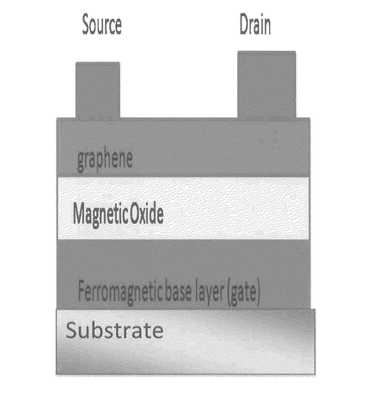
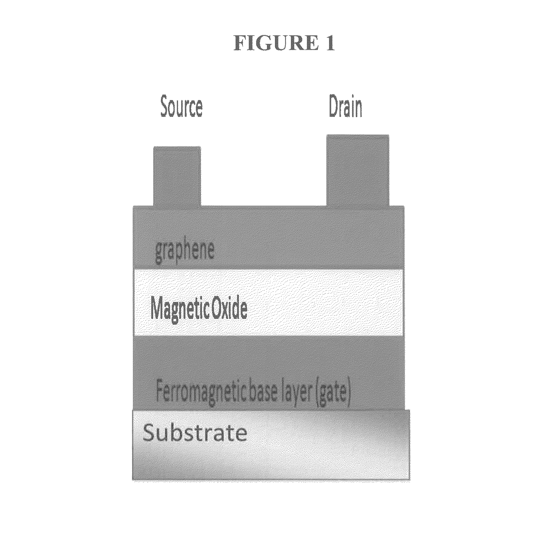
The invention is a new type of spin valve or spin-FET that uses graphene deposited on a magnetically polarizable electrically insulating or semiconducting substrate. The substrate's polarization results in polarization of the transition metal ions in the magnetic oxide at both the top and bottom interfaces, which in turn leads to polarization of the graphene valence / conduction band electrons. The spin-FET operates by gating the bottom base ferromagnetic layer, separated from the graphene conduction channel by a dielectric oxide. The non-local resistance of the spin-FET is dependent on the polarization of the graphene and the source and drain electrodes. The invention provides a better performance than conventional graphene-based spin valves due to the formation of magnetic polarons and the relatively few phonon-mediated decay pathways. No applied external magnetic field is required to maintain polarization of the graphene electrons, as the device should operate at remanance.

Problems solved by technology

For these reasons—substrate phonon interference and grain-boundary densities, the performance (i.e., non-local resistance) of conventional graphene-based spin valves at room temperature has been disappointingly poor for practical device applications.

Method used


Image

  • Coherent spin field effect transistor
  • Coherent spin field effect transistor
  • Coherent spin field effect transistor

Examples


example

[0025]In order to prepare a coherent spin-FET of the invention, a sapphire (aluminum oxide (0001)) substrate is prepared for deposition. An electron beam evaporator may be used to reduce movement between chambers and improve productivity, switching in various targets for deposition. Thus, a fifty angstrom layer of cobalt may be deposited under conventional conditions on the substrate at 750° K in UHV. This deposition is followed by an oxidation anneal at 1000° K which results in surface segregation of dissolved oxygen and the development of a thin layer of Co3O4(111) (may be 2-5 ML thick). Graphene (2 or 3 ML) is deposited on the Co3O4 using molecular beam epitaxy at 1000° K, yielding a macroscopically continuous graphene film of approximately 3 ML thickness. Graphene may also be deposited via CVD and PVD processes, as disclosed, but MBE is preferred, not only because of the fine control and developed information for this method, but because it is compatible with the other process s...


PUM


Abstract

A coherent spin field effect transistor is provided by depositing a ferromagnetic base like cobalt on a substrate. A magnetic oxide layer is formed on the cobalt by annealing at temperatures on the order of 1000° K to provide a few monolayer thick layer. Where the gate is cobalt, the resulting magnetic oxide is Co3O4(111). Other magnetic materials and oxides may be employed. A few ML field of graphene is deposited on the cobalt (III) oxide by molecular beam epitaxy, and a source and drain are deposited of base material. The resulting device is scalable, provides high on / off rates, is stable and operable at room temperature and easily fabricated with existing technology.

Description

[0001]The subject matter of this patent application was developed without federal or state funding. Although both inventors named herein are the beneficiaries of support from various corporate organizations, and are employed by Universities at which they work on subject matter including the development and characterization of materials formed by the direct growth of graphene on various substrates, no University time, compensation or apparatus was employed, involved or relied on in the development of the subject matter disclosed and claimed herein.BACKGROUND OF THE INVENTION[0002]1. Field of the Invention[0003]The present invention relates to the development of a non-local spin valve, sometimes referred to as a spin field effect transistor, or spin-FET. Spin-FETS that can be operated at ambient temperatures offer the advantages of greater data storage in less space, with a reduced power consumption, and high sensitivity. Spin-FETS offer non-volatile solid state data storage the does ...

Claims


Application Information

Patent Timeline
Patent Type & Authority Patents(United States)
IPC IPC(8): H01L21/02H10N52/01
CPCH01L29/66742H01L29/78603H01L29/78684H01L29/4908H01L29/1606H01L29/66984H01L43/14H01L29/78391H01L29/7869H10N52/01
Inventor KELBER, JEFFRYDOWBEN, PETER
Owner QUANTUM DEVICES
Learn More