Semiconductor device and method for producing same

a semiconductor and gate insulating film technology, applied in the direction of semiconductor devices, electrical devices, transistors, etc., can solve the problem of very high electric field intensity to be applied to gate insulating films, and achieve the effect of preventing dielectric breakdown and reducing electric field intensity

Inactive Publication Date: 2014-06-10
PANASONIC CORP
View PDF25 Cites 10 Cited by
  • Summary
  • Abstract
  • Description
  • Claims
  • Application Information

AI Technical Summary

Benefits of technology

[0016]According to an embodiment of the present invention, a thicker gate insulating film is arranged on the corner side surfaces located at corner portions of the trench, as compared with that on the main side surfaces, and it is therefore possible to reduce the electric field intensity occurring at the corner portions of the trench, thereby preventing dielectric breakdown.
[0017]According to a method for manufacturing a semiconductor device of one embodiment of the present invention, even if the trench is miniaturized, a thicker gate insulating film can be formed on the corner side surfaces of the trench, as compared with that on the main side surfaces, without complicating the manufacturing process.

Problems solved by technology

However, a problem with MISFETs of the trench gate structure is that the electric field intensity to be applied to the gate insulating film is very high.

Method used


Image

  • Semiconductor device and method for producing same
  • Semiconductor device and method for producing same
  • Semiconductor device and method for producing same

Examples


first embodiment

Manufacturing Method of First Embodiment

[0121]Next, referring to the drawings, an example of a method for manufacturing a semiconductor device of the present embodiment will be described.

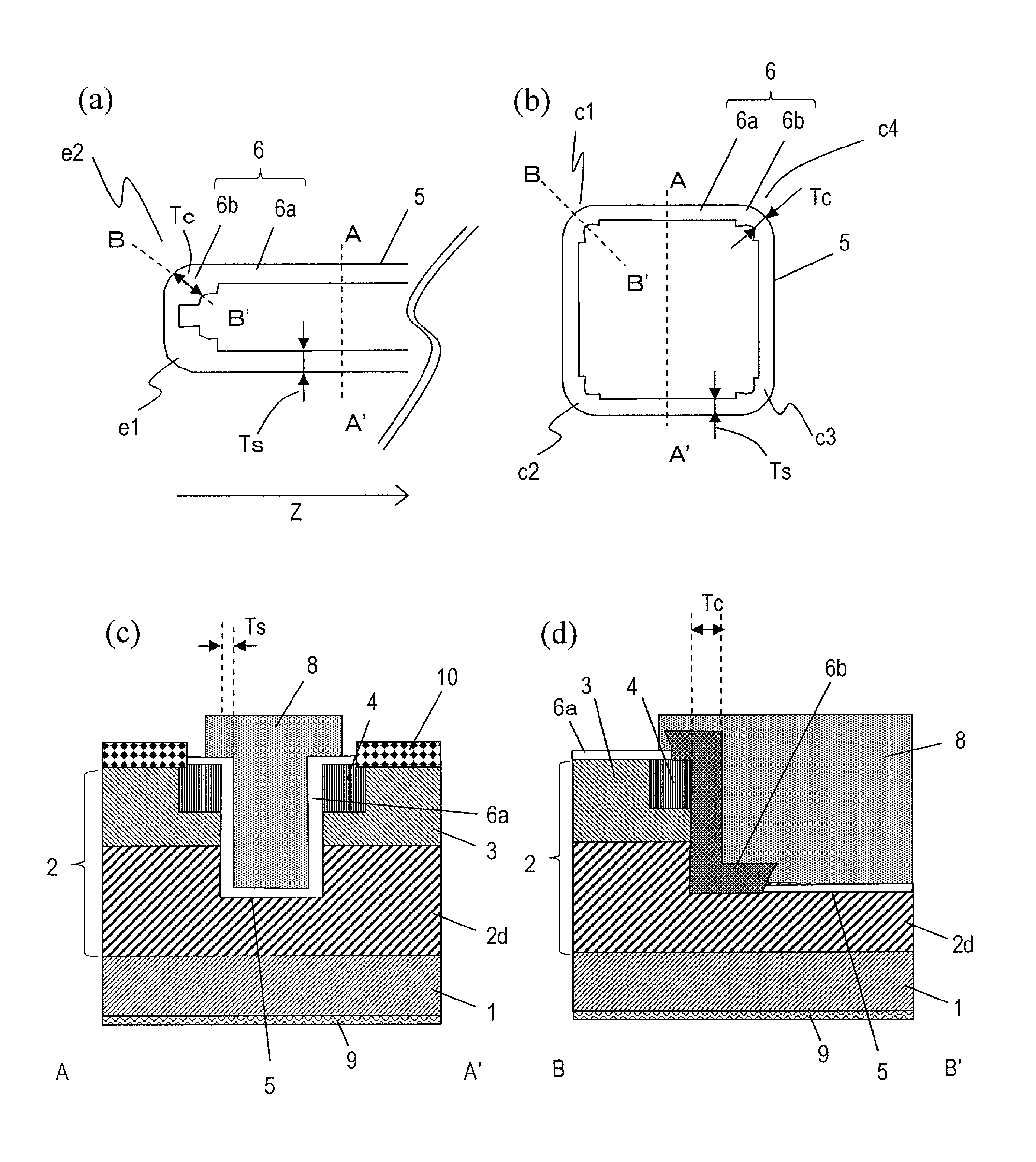
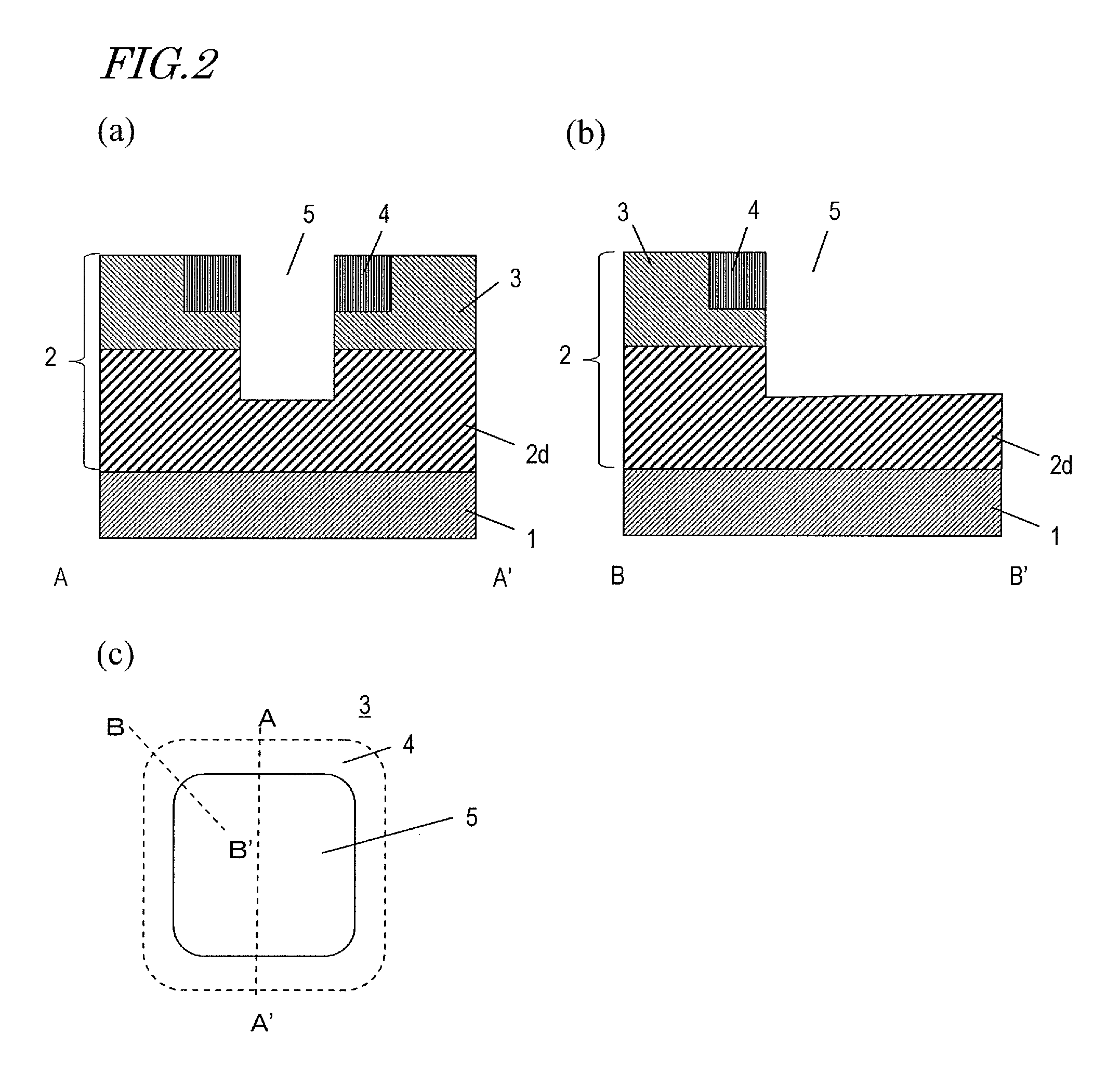
[0122]FIGS. 2 to 8 are diagrams each illustrating a method for manufacturing a semiconductor device of the present embodiment. In each figure, (a) and (b) are cross-sectional views taken along line A-A′ and line B-B′, respectively, of FIGS. 1(a) and 1(b), and (c) is a plan view of the trench 5. In the present embodiment and embodiments to follow, a portion of the plan view of the trench 5 formed by stripe-shaped cells is omitted.

[0123]First, as shown in FIGS. 2(a) to 2(c), the silicon carbide layer 2 including the drift region 2d of the first conductivity type (herein, n type) and the body region 3 of the second conductivity type (herein, p type) is obtained on the principal surface of the substrate 1, as in a conventional process. Then, the source region 4 is formed in the body region 3. After an a...

second embodiment

Manufacturing Method of Second Embodiment

[0161]Next, referring to the drawings, an example of a method for manufacturing a semiconductor device of the present embodiment will be described.

[0162]FIGS. 10 to 17 are diagrams each illustrating a method for manufacturing a semiconductor device of the present embodiment. In each figure, (a) and (b) are cross-sectional views taken along line A-A′ and line B-B′, respectively, of FIGS. 9(a) and 9(b), and (c) is A plan view of the trench 5.

[0163]First, as shown in FIGS. 10(a) to 10(c), the silicon carbide layer 2 including the drift region 2d of the first conductivity type (herein, n type) and the body region 3 of the second conductivity type (herein, p type) is obtained on the principal surface of the substrate 1, as in a conventional process. Then, the source region 4 is formed in the body region 3. After an annealing treatment is performed to activate the source region 4, the trench 5 is formed in the silicon carbide layer 2. The method fo...

third embodiment

Manufacturing Method of Third Embodiment

[0184]Next, referring to the drawings, an example of a method for manufacturing a semiconductor device of the present embodiment will be described.

[0185]FIGS. 19 to 27 are diagrams each illustrating a method for manufacturing a semiconductor device of the present embodiment. In each figure, (a) and (b) are cross-sectional views taken along line A-A′ and line B-B′, respectively, of FIGS. 18(a) and 18(b), and (c) is a plan view of the trench 5.

[0186]First, as shown in FIGS. 19(a) to 19(c), the silicon carbide layer 2 including the drift region 2d of the first conductivity type (herein, n type) and the body region 3 of the second conductivity type (herein, p type) is obtained on the principal surface of the substrate 1, as in a conventional process. Then, the source region 4 is formed in the body region 3. After an annealing treatment is performed to activate the source region 4, the trench 5 is formed in the silicon carbide layer 2. The method f...


PUM


Abstract

A semiconductor device according to an embodiment of the present invention includes: a semiconductor layer 2 of a wide band gap semiconductor arranged on a principal surface of a substrate 1; a trench 5 arranged in the semiconductor layer and including a bottom surface, a plurality of main side surfaces, and a plurality of corner side surfaces each connecting together two adjacent main side surfaces; a gate insulating film 6 arranged on the bottom surface, the main side surfaces and the corner side surfaces of the trench 5; and a gate electrode 8 arranged in the trench, wherein the semiconductor layer includes a drift region 2d of a first conductivity type, and a body region 3 of a second conductivity type arranged on the drift region; the trench runs through the body region 3 and has the bottom surface inside the drift region; the corner side surfaces of the trench do not have a depressed portion; the gate insulating film 6 is thicker on the corner side surfaces of the trench than on the main side surfaces of the trench; and a portion of the gate insulating film 6 that is located on the corner side surfaces is a first insulating layer 6b, and a portion of the gate insulating film 6 that is located on the main side surfaces is a second insulating layer 6a.

Description

TECHNICAL FIELD[0001]The present application relates to an MIS (Metal Insulator Semiconductor) type semiconductor device having a trench gate structure using a wide band gap semiconductor, and a method for manufacturing the same.BACKGROUND ART[0002]Wide band gap semiconductors have been applied to various types of semiconductor devices, such as power elements (also referred to as “power devices”), environmental resistance elements, high-temperature operation elements, and high-frequency elements. Among others, applications to power devices, such as switching elements and rectifier elements, have been drawing public attention.[0003]Typical switching elements of power devices include field effect transistors, such as metal-insulator-semiconductor field effect transistors (hereinafter, “MISFETs”) and metal-semiconductor field effect transistors (hereinafter, “MESFETs”). Such a switching element can be switched, based on the voltage applied between the gate electrode and the source elec...

Claims


Application Information

Patent Timeline
Patent Type & Authority Patents(United States)
IPC IPC(8): H01L29/20H01L29/16H01L29/739H01L29/06H01L29/78H01L21/28H01L29/66H01L29/423
CPCH01L29/4238H01L29/66045H01L29/66068H01L29/4236H01L29/7397H01L29/66734H01L29/1608H01L29/2003H01L21/28008H01L29/42368H01L29/7813H01L29/7827H01L29/1602H01L29/0607
Inventor KUDOU, CHIAKI
Owner PANASONIC CORP
Why Eureka
Try Eureka