Method for the reduction of graphene film thickness and the removal and transfer of epitaxial graphene films from SiC substrates

a graphene film and epitaxial technology, applied in the field of graphene and polycrystalline diamond films, can solve the problems of low efficiency of graphene-based electronics mass production, and large thickness of epitaxial graphene films, and achieves easy fabrication of electronic or optoelectronic devices, easy characterization of graphene layers, and simple oxygen reduction process

Active Publication Date: 2014-06-17
THE UNITED STATES OF AMERICA AS REPRESENTED BY THE SECRETARY OF THE NAVY
View PDF7 Cites 29 Cited by
  • Summary
  • Abstract
  • Description
  • Claims
  • Application Information

AI Technical Summary

Benefits of technology

[0008]The present invention enables the removal and transfer of graphene, graphane and / or graphene oxide films from one substrate to another. This enables the graphene to be removed from a donor substrate that is suitable for large size-scale production, such as SiC wafers or metal catalyst films / foils, and then subsequently transferred onto arbitrary handle substrates that are more desirable for device fabrication for reasons such as, but not limited to, cost efficiency, ease in device fabrication or for improved substrate attributes such as flexibility, optical transmission, thermal conductivity or improved electrical isolation from the substrate. This would also enable the transfer of graphene films to optoelectronic or electronic devices where the films may be used as a contact that is optically transparent and highly conductive or one that is electrically and thermally conductive.
[0010]Once transferred, the graphene films are amenable to a simple oxygen reduction process for etching, enabling easy fabrication of electronic or optoelectronic devices. Further, since the graphene films are typically inert in all but oxygen or hydrogen atmospheres, it is possible to chemically undercut material below the transferred graphene layers, or to transfer the films to a previously undercut substrate, thereby leaving behind suspended graphene films. This enables easier characterization of graphene layers by allowing the samples to be both free standing and transferred to substrates that are more amenable to the characterization method of interest.

Problems solved by technology

Due to the difficulty in mass producing graphene films, it remains one of the most expensive materials known, with costs of over $1000 for a micron-sized sample as of April 2008.
Currently, the most widely used method is the exfoliation process from a Kisch or natural graphite substrate; however, reproducibility in the number of layers, uniformity in the layer thickness and layer widths make this method the least promising for mass production of graphene-based electronics.
Procedures for the transfer of these films in solution have been developed, however, the thickness of these films tends to be very large and the transfer process is destructive, requiring dissolving the metal catalyst for each sample created.
This process is capable of creating large-area graphene films, with the limitation derived simply by the size of the largest available SiC substrates (currently, substrates up to 4″ in diameter are available commercially).
Due to the large number of layers on the carbon face, it can be difficult to modulate the conductivity of the carriers participating in the transport in the graphene layers through the use of field-effect gate modulation.
While the above devices and applications hold very high promise, all of the current processes for creating thin graphene layers lack the ability to create large-area graphene films of a few layers on a substrate amenable to cost-effective device fabrication and operation.
There is no control over the graphene thickness or uniformity removed and the transfer procedure involves repeatedly placing the tape and graphene onto the desired substrate and peeling away, leaving graphene films with non-uniform thicknesses, morphologies, sizes and shapes.
Further, this process is not amenable to a single-flip process and therefore only the exposed graphene surface may be accessed.
There are many difficulties with this transfer procedure.
First, it is a destructive technique, involving the etching of the underlying substrate, which is costly.
For epitaxial graphene grown on SiC this process is not possible, as SiC is not known to be readily soluble in any solution in its bulk form.
Second, this process involves transferring of a graphene film in solution by floating the film on the solution surface and then pulling the handle substrate up through the solution, catching the graphene film on the substrate as it is removed from the solution.
This process would presumably induce wrinkling, folding or tearing of the graphene films during the transfer process.

Method used


Image

  • Method for the reduction of graphene film thickness and the removal and transfer of epitaxial graphene films from SiC substrates
  • Method for the reduction of graphene film thickness and the removal and transfer of epitaxial graphene films from SiC substrates
  • Method for the reduction of graphene film thickness and the removal and transfer of epitaxial graphene films from SiC substrates

Examples


Embodiment Construction

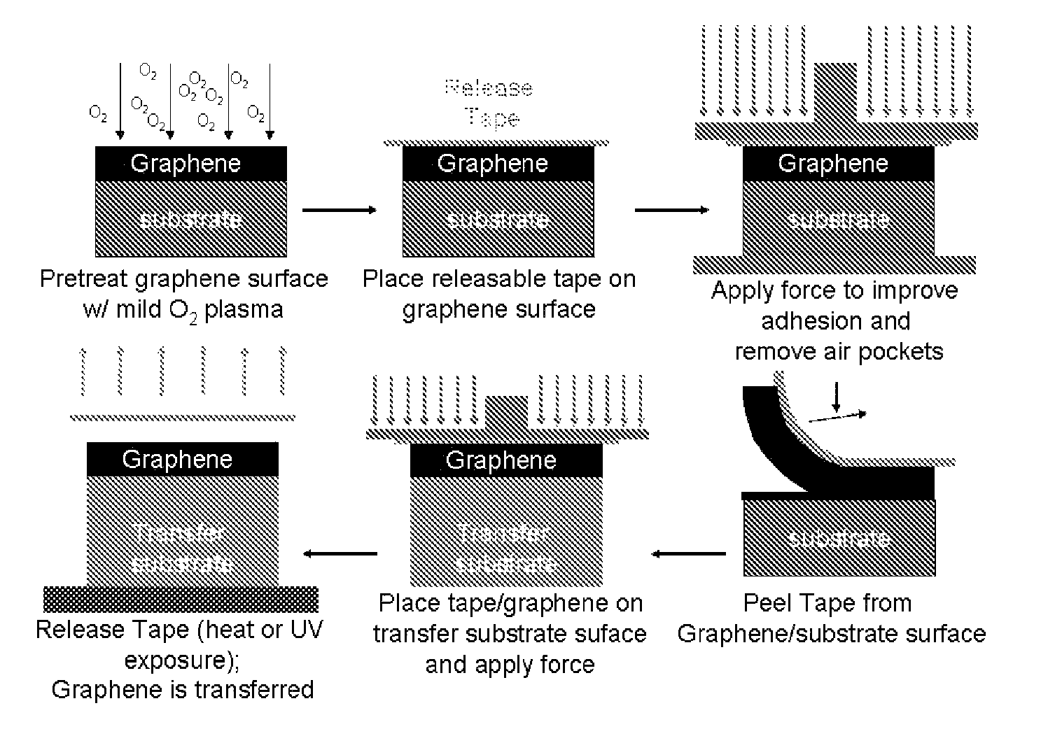
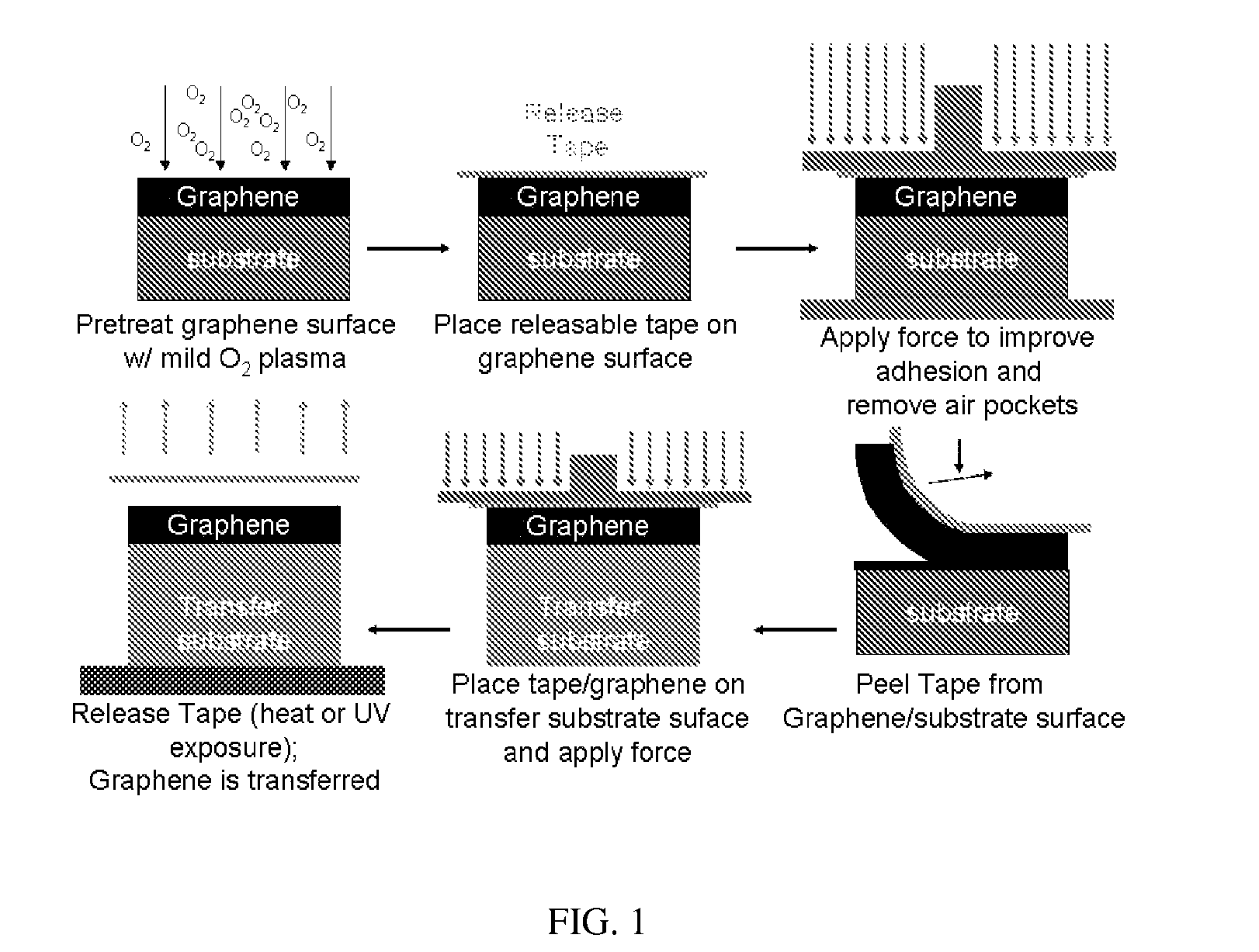
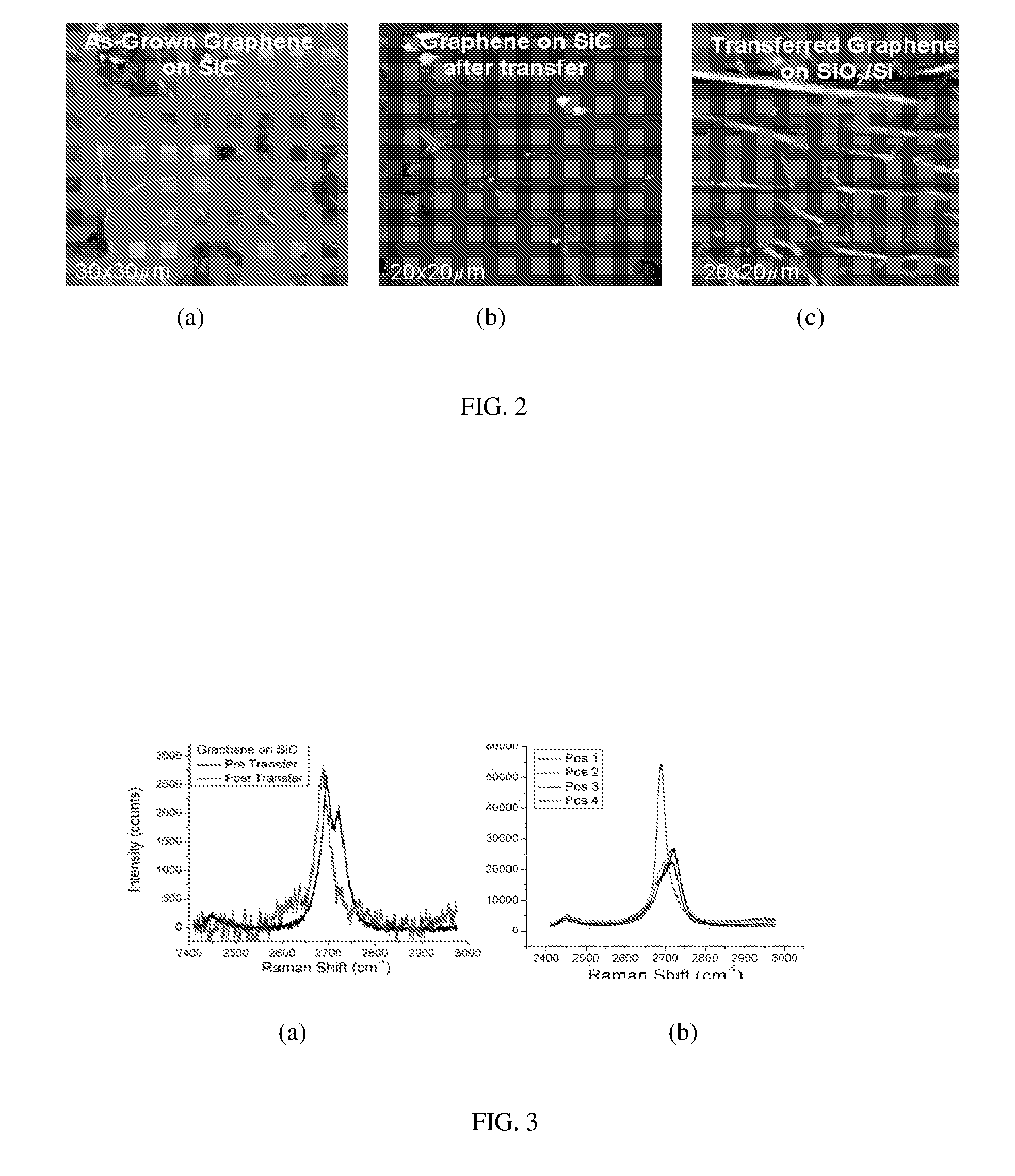
[0017]The present invention is directed towards a method enabling the transfer of large area graphene films from a donor substrate (e.g. SiC) to a handle substrate (e.g. silicon). The method involves three highly beneficial processes for the removal, reduction in layer thickness (number of graphene layers) and transfer of large areas of epitaxial graphene films from silicon carbide (SiC) substrates. Graphene is the name given to single sheets of graphitic carbon, which has been shown recently to possess electrical properties that are highly desirable, such as high carrier mobilities (1,000-200,000 cm2 / Vs), ballistic electron transport, and quantized optical transmission. There are primarily three methods for the creation of graphene-based devices (including both electronic, sensing, and MEMS devices). Graphene on SiC and metal-catalyzed graphene both offer the ability to create large-scale (>wafer scale) graphene films that may then be manipulated using the processes described here ...


PUM

PropertyMeasurementUnit
areaaaaaaaaaaa
temperaturesaaaaaaaaaa

Abstract

A method for reducing graphene film thickness on a donor substrate and transferring graphene films from a donor substrate to a handle substrate includes applying a bonding material to the graphene on the donor substrate, releasing the bonding material from the donor substrate thereby leaving graphene on the bonding material, applying the bonding material with graphene onto the handle substrate, and releasing the bonding material from the handle substrate thereby leaving the graphene on the handle substrate. The donor substrate may comprise SiC, metal foil or other graphene growth substrate, and the handle substrate may comprise a semiconductor or insulator crystal, semiconductor device, epitaxial layer, flexible substrate, metal film, or organic device.

Description

[0001]The present application is a non-provisional application that claims the benefit of provisional patent application Ser. No. 61 / 237,342 to Caldwell et al., filed Aug. 27, 2009 entitled “METHOD FOR THE REDUCTION OF GRAPHENE FILM THICKNESS AND THE REMOVAL AND TRANSFER OF EPITAXIAL GRAPHENE FILMS FROM SiC SUBSTRATES,” the entire contents of which is incorporated herein by reference.FIELD OF THE INVENTION[0002]The present invention relates generally to graphene and polycrystalline diamond films and more specifically to the transfer of epitaxial graphene films from the SiC growth substrate onto arbitrary substrates.BACKGROUND OF THE INVENTION[0003]Graphene is the name denoted to a single sheet (1 atom thick) of sp2-bonded carbon atoms. Effectively this is a single sheet of graphitic carbon. However, the term graphene has also come to be used to describe in a more general sense thin films (1-40 layers) of sp2-bonded carbon under the auspices of discussions of single layer interaction...

Claims


Application Information

Patent Timeline
Patent Type & Authority Patents(United States)
IPC IPC(8): B32B37/26B44C1/24B32B37/02B32B38/10B44C1/17B32B37/12B44C3/08B29C65/48
CPCC01B31/0438B82Y30/00B82Y40/00C01B31/043C01B31/0484C01B32/23C01B32/194
Inventor CALDWELL, JOSHUA D.HOBART, KARL D.ANDERSON, TRAVISKUB, FRANCIS J.
Owner THE UNITED STATES OF AMERICA AS REPRESENTED BY THE SECRETARY OF THE NAVY
Why Eureka
Try Eureka