Demodulation pixel with daisy chain charge storage sites and method of operation therefor

a technology of demodulation pixels and storage sites, applied in the field of demodulation pixels with daisy chain charge storage sites and methods of operation therefor, can solve the problems of insufficient space in the demodulation region to implement the design of more than, strong impede the implementation of demodulation pixels with more than two sampling storage sites, and mismatch between samples, etc., to achieve the effect of strong reduction of mismatch between samples

Active Publication Date: 2014-06-24
AMS SENSORS SINGAPORE PTE LTD
View PDF15 Cites 9 Cited by
  • Summary
  • Abstract
  • Description
  • Claims
  • Application Information

AI Technical Summary

Benefits of technology

[0016]Furthermore, embodiments can reduce the problem of mismatch of the different sampling channels. The behavior mismatch of the different samples is mainly caused by the different directions of the photocharge transfer for different samples. Here, all samplings can be performed in the same direction of the semi-conductor lattice. In other words, the transfer direction does not have to be changed and, hence, the mismatch between samples is strongly reduced.

Problems solved by technology

So far, the implementation of demodulation pixels with more than two sampling storage sites were strongly hindered by the integrated circuit design layout rules restrictions.
Since the demodulation region is preferably quite small compared to photo-sensitive area, in most cases the demodulation region does not offer enough space to implement the design of more than two sampling stages.
The behavior mismatch of the different samples is mainly caused by the different directions of the photocharge transfer for different samples.

Method used


Image

  • Demodulation pixel with daisy chain charge storage sites and method of operation therefor
  • Demodulation pixel with daisy chain charge storage sites and method of operation therefor
  • Demodulation pixel with daisy chain charge storage sites and method of operation therefor

Examples


Embodiment Construction

[0036]The following discussion concerns a sensor with a p-doped substrate in which electrons are the useful photo-generated charge carriers. All considerations can also be done for n-doped material, with holes as carriers of information. In this case the voltages applied to gates and / or diffusions would be reversed.

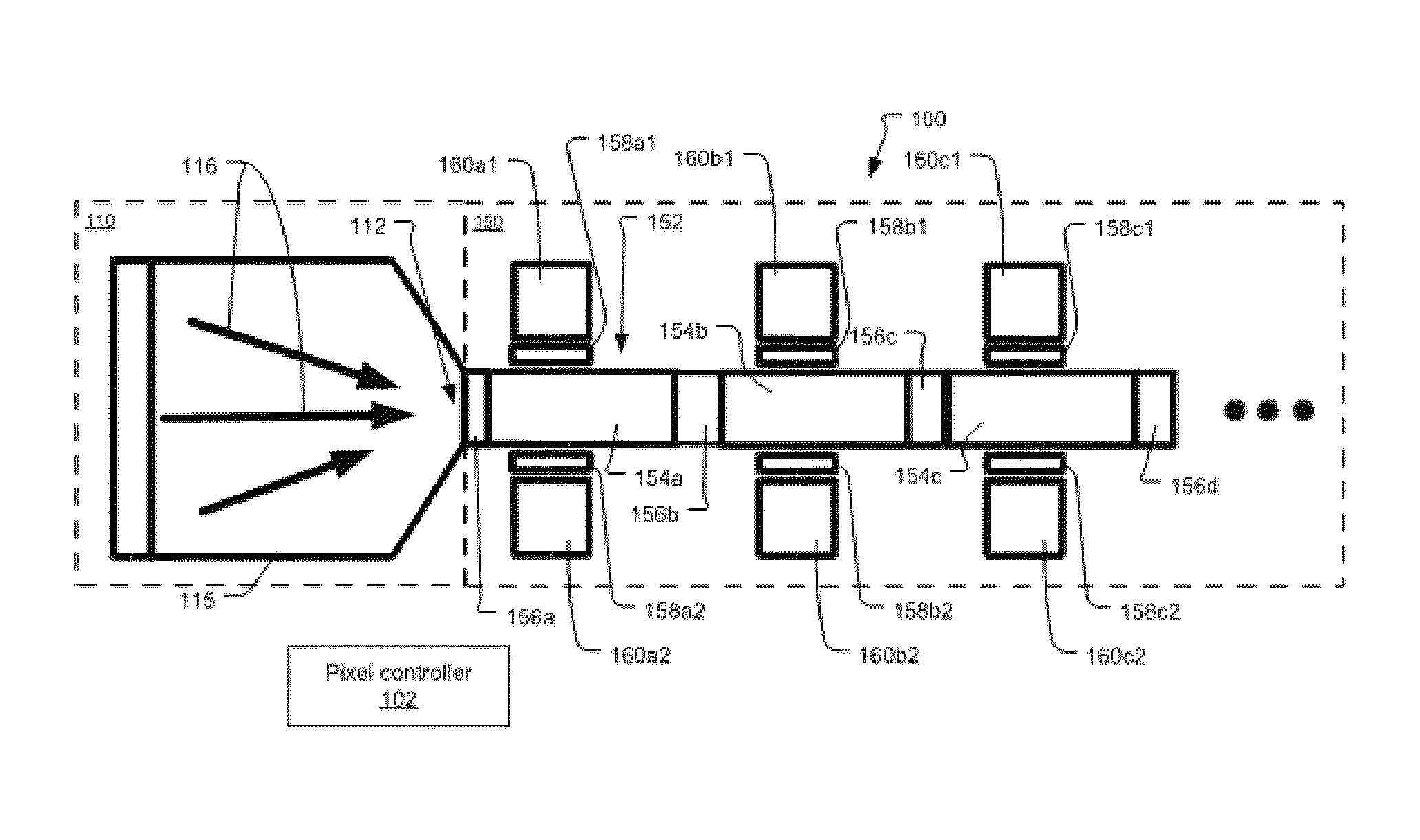
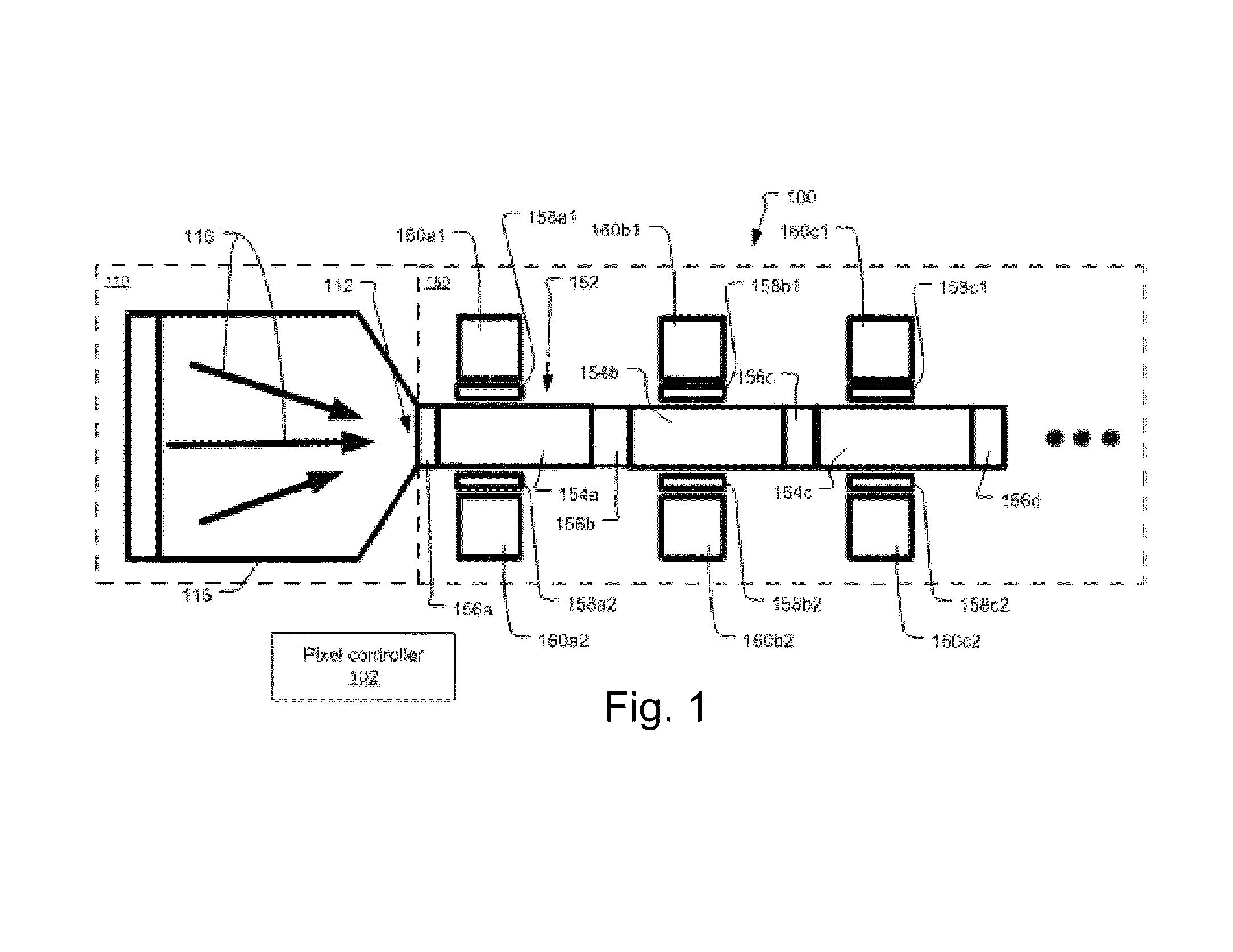
[0037]FIG. 1 shows a demodulation pixel 100 embodied in a semiconductor substrate that has been constructed according to the principals of the present invention.

[0038]The pixel 100 comprises a photosensitive region 110. This is typically characterized by a portion of the semiconductor substrate that receives incoming light or other radiation and is not otherwise shielded by opaque layers, such as metal, layers. The photosensitive region 110 has a photocharge transport area 115 that moves the photocharges to a pickup point 112, typically at one end of the transport area 115.

[0039]The photocharge transport area 115 transports the photocharges to the pickup point 112 typical...


PUM


Abstract

A demodulation pixel architecture allows for demodulating an incoming modulated electromagnetic wave, normally visible or infrared light. It is based on a charge coupled device (CCD) line connected to a drift field structure. The drift field is exposed to the incoming light. It collects the generated charge and forces it to move to the pick-up point. At this pick-up point, the CCD element samples the charge for a given time and then shifts the charge packets further on in the daisy chain. After a certain amount of shifts, the multiple charge packets are stored in so-called integration gates, in a preferred embodiment. The number of integration gates gives the number of simultaneously available taps. When the cycle is repeated several times, the charge is accumulated in the integration gates and thus the signal-to-noise ratio increases. The architecture is flexible in the number of taps. A dump node can be attached to the CCD line for dumping charge with the same speed as the samples are taken. Different implementations are described herein, which allow for smaller design or faster speed. The pixel structure can be exploited for e.g. 3D time-of-flight imaging. Both heterodyne and homodyne measurements are possible. Due to the highly-efficient charge transport enabled by static drift fields in the photo-sensitive region and small-sized gates in the CCD chain, high frequency bandwidth from just a few Hertz (Hz) up to greater GHz is supported. Thus, the pixel allows for highly-accurate optical distance measurements. Another possible application of this pixel architecture is fluorescence lifetime imaging microscopy (FLIM), where short laser pulses for triggering the fluorescence have to be suppressed.

Description

RELATED APPLICATIONS[0001]This application claims the benefit under 35 USC 119(e) of U.S. Provisional Application No. 61 / 092,548, filed on Aug. 28, 2008, which is incorporated herein by reference in its entirety.BACKGROUND OF THE INVENTION[0002]The demodulation of modulated light at the pixel level requires the switching of a photo-generated charge current. While possible to handle both electron as well as hole currents, the common methods today use the photo-generated electron currents. This choice is largely due to the higher mobility of electrons in the semiconductor material. Some pixel architectures do the necessary signal processing based on the photo-current while others work directly in the charge domain.[0003]All of the pixel architectures transfer photocharges through the photo-sensitive detection region to a subsequent storage area or to a subsequent processing unit. In the case of charge-domain based pixel architectures, the photocharges are generally transferred to an i...

Claims


Application Information

Patent Timeline
Patent Type & Authority Patents(United States)
IPC IPC(8): H04N3/14H04N5/335H01L27/148G01S7/4914H04N5/372
CPCH01L27/14603H01L27/14609G01S7/4914H04N25/00H04N25/70
Inventor LEHMANN, MICHAELBUTTGEN, BERNHARD
Owner AMS SENSORS SINGAPORE PTE LTD
Why Eureka
Try Eureka