Photoelectric conversion device and energy conversion layer for photoelectric conversion device

a conversion device and photoelectric technology, applied in semiconductor devices, nanotechnology, nanotechnology, etc., to achieve the effects of reducing the cost of the conversion device, and reducing the weight of the photoelectric conversion devi

Inactive Publication Date: 2014-07-22
SEMICON ENERGY LAB CO LTD
View PDF17 Cites 0 Cited by
  • Summary
  • Abstract
  • Description
  • Claims
  • Application Information

AI Technical Summary

Benefits of technology

[0008]In view of the above, it is an object to provide a novel photoelectric conversion device in which energy of light can be effectively utilized and performance can be improved. In addition, it is an object to provide a photoelectric conversion device in which energy of visible light with a shorter wavelength than ultraviolet light can be effectively utilized. Moreover, it is an object to provide an energy conversion layer for a photoelectric conversion device which can improve the performance of the photoelectric conversion device.
[0037]In the above structure, the photoelectric conversion element and the energy conversion layer can be provided over one substrate. When the photoelectric conversion element and the energy conversion layer are provided over one substrate, as compared to the case where the photoelectric conversion element and the energy conversion layer are provided over different substrates, cost down, downsizing, and reduction in weight of the photoelectric conversion device can be achieved. In addition, optical loss due to substrates, which may be generated in the case where the photoelectric conversion element and the energy conversion layer are provided over different substrates, can be reduced.
[0038]It is possible to provide a novel photoelectric conversion device in which energy of light can be effectively utilized and performance such as conversion efficiency can be improved. In particular, it is possible to provide a photoelectric conversion device in which spectral sensitivity and quantum efficiency of visible light with a shorter wavelength than ultraviolet light can be increased and energy of light with a short wavelength can be effectively utilized. Moreover, it is possible to provide an energy conversion layer for a photoelectric conversion device which can improve the performance of the photoelectric conversion device.

Problems solved by technology

However, even when a photoelectric conversion layer absorbs light with a short wavelength whose energy is higher than that of the energy band gap of the photoelectric conversion layer, energy which is not within the energy range of the energy band gap of the photoelectric conversion layer is released as thermal energy, and cannot be taken out as power of a solar cell.

Method used


Image

  • Photoelectric conversion device and energy conversion layer for photoelectric conversion device
  • Photoelectric conversion device and energy conversion layer for photoelectric conversion device
  • Photoelectric conversion device and energy conversion layer for photoelectric conversion device

Examples


embodiment 1

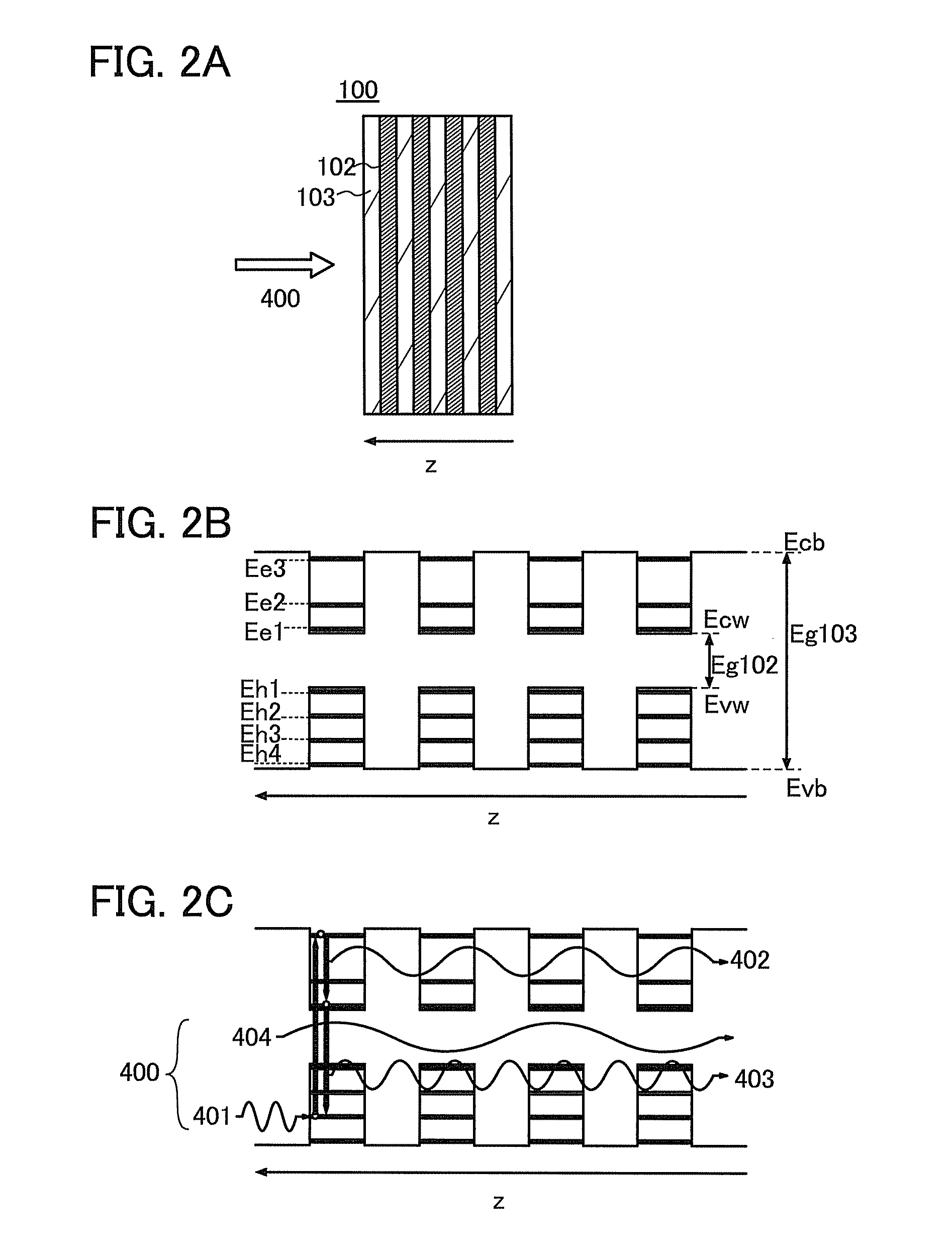
[0049]In this embodiment, an example of a structure of a photoelectric conversion device and an example of a structure of an energy conversion layer according to an embodiment of the disclosed inversion will be described with reference to FIGS. 1A and 1B and FIGS. 2A to 2C.

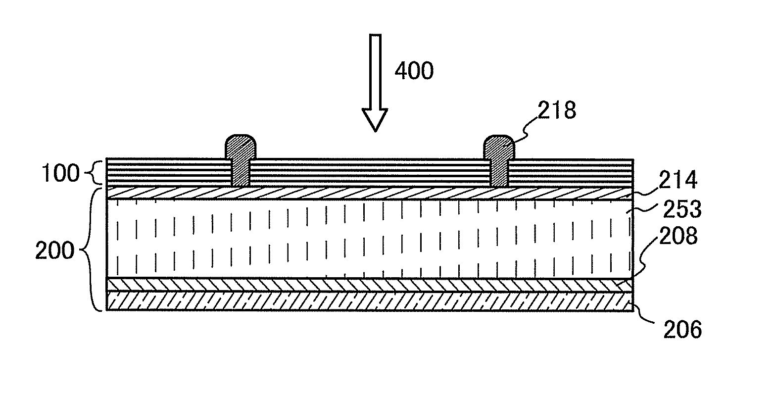
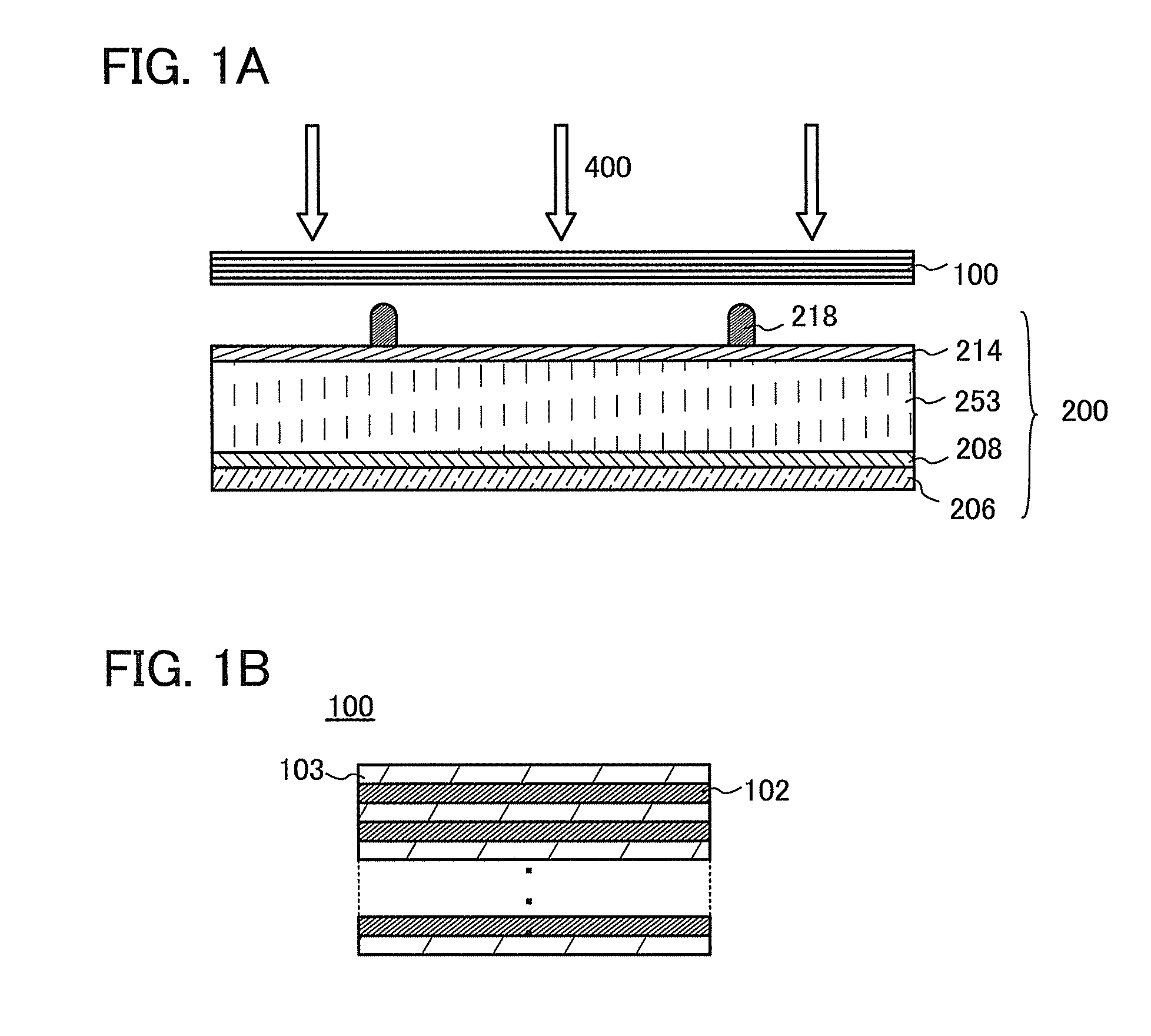
[0050]FIG. 1A is a cross-sectional schematic view illustrating an example of a photoelectric conversion device. The photoelectric conversion device includes a photoelectric conversion element 200 and an energy conversion layer 100. The energy conversion layer 100 is provided on the light-receiving side of the photoelectric conversion element 200. Incident light 400 enters a photoelectric conversion layer 253 included in the photoelectric conversion element 200 through the energy conversion layer 100.

[0051]The photoelectric conversion element 200 includes a first electrode 206, the photoelectric conversion layer 253, and a second electrode 218. In addition, the photoelectric conversion element 200 includes a first ...

embodiment 2

[0075]In this embodiment, an example of a structure of an energy conversion layer for a photoelectric conversion device according to an embodiment of the disclosed inversion will be described with reference to FIG. 3.

[0076]FIG. 3 is a cross-sectional schematic view illustrating, by enlarging, an example of an energy conversion layer 100 used in a photoelectric conversion device. The energy conversion layer 100 includes a first unit 104 and a second unit 105. The first unit 104 includes a plurality of first layers 102a with a first thickness and a plurality of second layers 103a with a second thickness, and the first layer 102a and the second layer 103a are alternately stacked. The second unit 105 includes a plurality of third layers 102b with a third thickness and a plurality of fourth layers 103b with a fourth thickness, and the third layer 102b and the fourth layer 103b are alternately stacked. Each of the plurality of first layers 102a is sandwiched between the second layers 103a...

embodiment 3

[0085]In this embodiment, an example of a structure of an energy conversion layer for a photoelectric conversion device according to an embodiment of the disclosed inversion will be described with reference to FIG. 4.

[0086]FIG. 4 is a perspective view illustrating an example of an energy conversion layer 100.

[0087]The energy conversion layer 100 includes a plurality of first layers 112 each having a longitudinal direction (a y direction in FIG. 4) and a lateral direction (a x direction in FIG. 4) and a second layer 113. Each of the plurality of first layers 112 is surrounded by the second layer 113 in a cross section in a lateral direction. The plurality of first layers 112 each having a longitudinal direction and a lateral direction are arranged at predetermined intervals in a thickness direction (also referred to as a vertical direction or a z direction in FIG. 4). The plurality of first layers 112 each having a longitudinal direction and a lateral direction are arranged at predet...


PUM


Abstract

A novel photoelectric conversion device in which energy of light can be effectively utilized and performance can be improved is provided. A photoelectric conversion device includes a photoelectric conversion element and an energy conversion layer provided on a light-receiving side of a photoelectric conversion layer included in the photoelectric conversion element. The energy conversion layer includes a plurality of first layers and a plurality of second layers. The first layer and the second layer are alternately stacked. The thickness of the first layer is greater than or equal to 0.5 nm and less than or equal to 10 nm, and the thickness of the second layer is greater than or equal to 0.5 nm and less than or equal to 10 nm. The second layer can be formed using a material having a larger energy band gap than that of a material used for the first layer.

Description

BACKGROUND OF THE INVENTION[0001]1. Field of the Invention[0002]An embodiment of the present invention relates to a photoelectric conversion device such as a solar cell.[0003]2. Description of the Related Art[0004]A photoelectric conversion device such as a solar cell has been actively researched and developed. The spectrum of the sunlight widely ranges from light with a short wavelength (such as ultraviolet light) to light with a long wavelength (such as infrared light). Energy of light with a short wavelength is higher than energy of light with a long wavelength. Therefore, when energy of light with a short wavelength can be efficiently utilized, the conversion efficiency of a solar cell can be improved.[0005]For example, it has been attempted to improve the conversion efficiency of a solar cell by using a wavelength conversion layer (e.g., Patent Document 1).REFERENCEPatent Document[0006][Patent Document 1] Japanese Published Patent Application No. H7-142752SUMMARY OF THE INVENTI...

Claims


Application Information

Patent Timeline
Patent Type & Authority Patents(United States)
IPC IPC(8): H01L31/06H01L31/054H01L31/055
CPCB82Y20/00B82Y10/00H01L21/02422H01L21/0245H01L21/02488H01L21/02507H01L21/02513H01L21/0262H01L31/035218H01L31/035236H01L31/0384H01L31/075H01L31/18Y02E10/548Y02E10/52H01L31/046H01L31/0352H01L31/035209H01L31/035227H01L31/04
Inventor ASAMI, YOSHINOBUYOKOI, TOMOKAZU
Owner SEMICON ENERGY LAB CO LTD
Why Eureka
Try Eureka