
Scanned UV-LED exposure device

a radiation exposure device and ultraviolet light technology, applied in the field of ultraviolet light emitting diodes (uvled) radiation exposure devices, can solve the problems of unstable uv light sources for the separated portions, large space occupation of the radiation exposure station, irregular scan speed, etc., to improve the use efficiency of energy sources and improve the uniformity of radiation exposure

Inactive Publication Date: 2014-08-19
NAT CENT UNIV
View PDF3 Cites 3 Cited by
  • Summary
  • Abstract
  • Description
  • Claims
  • Application Information

AI Technical Summary

Benefits of technology

The present invention provides a scanned UV-LED exposure device that can overcome problems of the prior art by having a large area and separated portions based exposure capability, and performing a scanned exposure task on the large object area based on a periodic manner by a fixed rate without needing stopping movement of the device. This results in improved uniformity of exposure and increased efficiency of energy usage. Additionally, the invention provides a scanned UV-LED exposure device with reduced volume, corresponding production space, energy consumption, and production cost, and improved production efficiency.

Problems solved by technology

In the past, an exposure station other than the ultraviolet-light emitting diode (UV-LED) system is quite space consuming, and so is a manufacturing assembly space involved with that.
This results in an irregular scan speed and thus an unstable UV light source for the separated portions.
Further, this exposure manner with respect to a single LED position may cause an insufficient radiant illumination and thus an unsatisfactory exposure uniformity, leading also to a low yield.
In addition, in such exposure task regime, the light source has to be kept being turned on, which results in a short UV light source lifetime.
Further, the light source has to be warmed in a preparation stage whenever the UV light source is turned on to use, making the light source hard to be controlled in its on / off states.

Method used


Image

  • Scanned UV-LED exposure device
  • Scanned UV-LED exposure device
  • Scanned UV-LED exposure device

Examples


Embodiment Construction

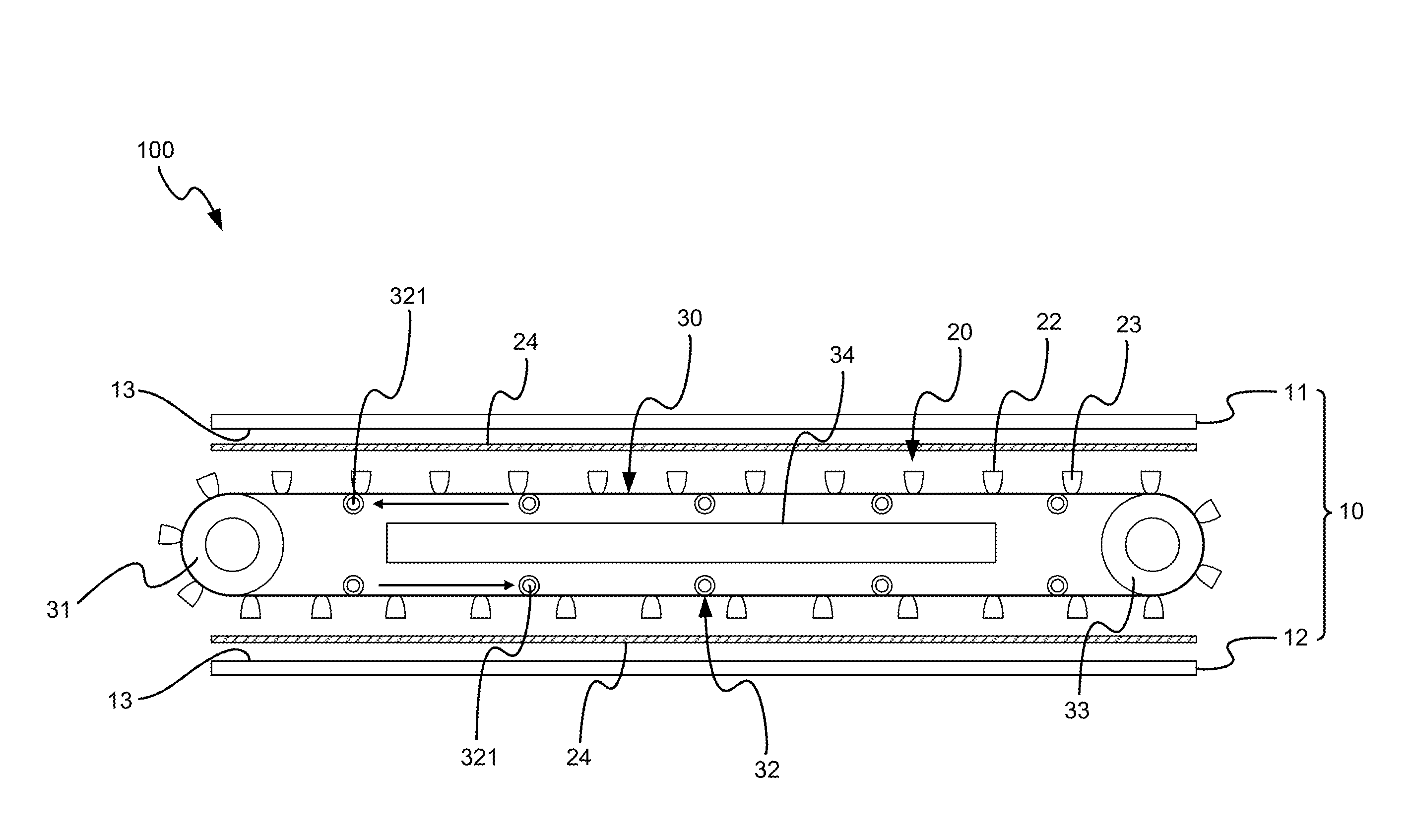
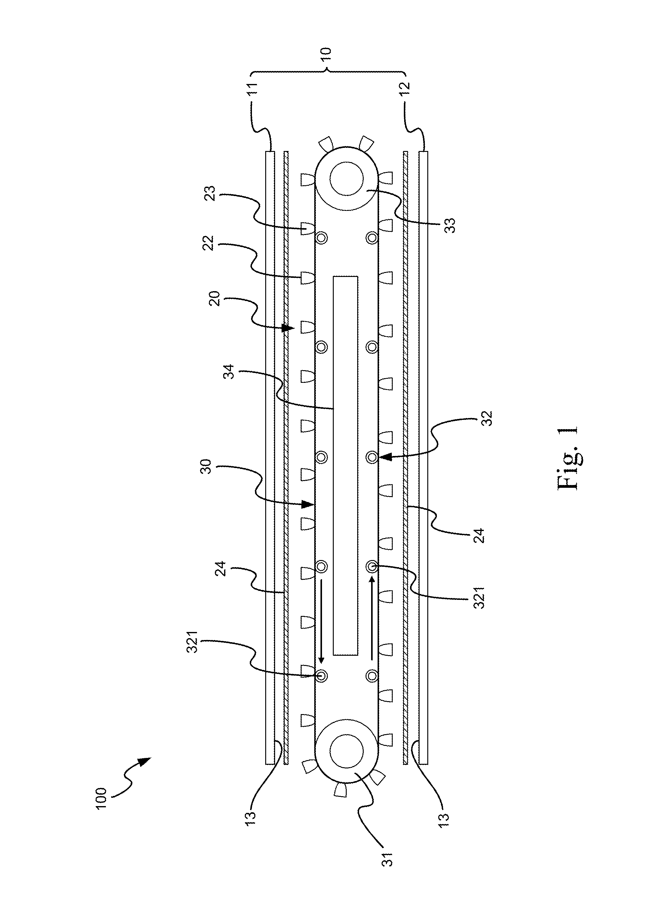
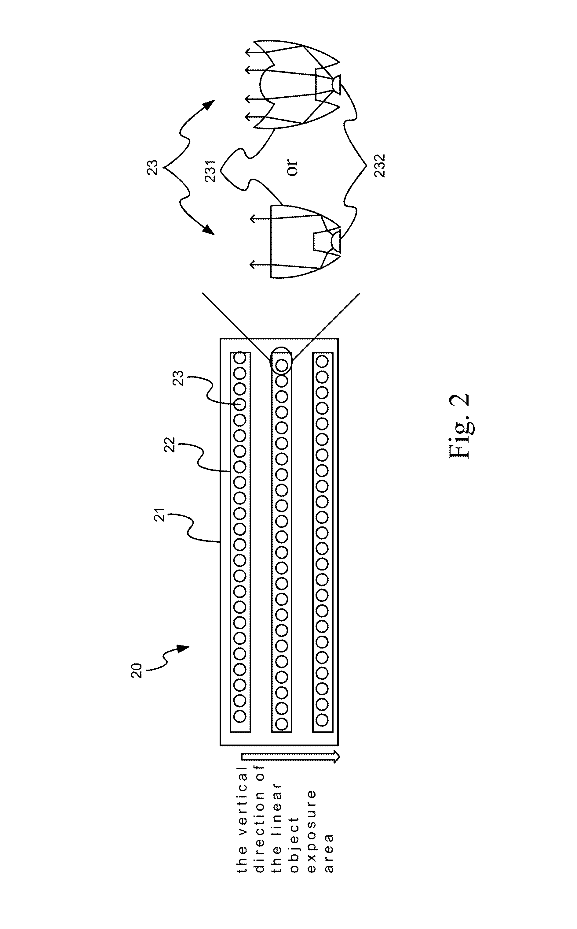
[0027]Referring assembly to FIG. 1 through FIG. 3, a schematic diagram of a structure of a scanned ultraviolet-light emitting diode (UV-LED) exposure device, a vertical view of a UV-LED illumination unit in a preferred embodiment and a vertical view of the UV-LED illumination unit in another preferred embodiment according to the present invention are shown, respectively.

[0028]As shown, the scanned UV-LED exposure device of the present invention is an LED exposure station having a large area and separated portions exposure capability, where a light source for exposure goes through a mask to illuminate an object exposure area.

[0029]The scanned UV-LED exposure device 100 comprises an exposure unit 10, a UV-LED illumination unit 20, and a periodic moving ring assembly 30,

[0030]The exposure unit 10 comprises a set of upper exposure station 11 and a lower exposure station 12, which are arranged with a distance therebetween. Each of the upper and lower exposure stations 11, 12 has a surfac...


PUM


Abstract

A scanned ultraviolet-light emitting diode (UV-LED) exposure device, exposing a large area by using a periodic UV-LED exposure light source with a fixed rate in an exposure task without a need of stopping movement of the device, so as to periodically repeat a use of an exposure light source to increase a use efficiency of the energy source, resulting in an improved uniformity of exposure, with the LEDs alternatively arranged policy, which further results in an improved yield. In addition, the overall design of the upper and lower exposure stations and the periodic moving ring assembly sufficiently employs the available space, and results in a reduced volume, a corresponding production space, energy consumption and production cost.

Description

FIELD OF THE INVENTION[0001]The present invention is related to a scanned ultraviolet-light emitting diode (UV-LED) exposure device, and particularly to an LED exposure device having a large area and separated portions based exposure capability, and more particularly to a scanned UV-LED exposure device performing a scanned exposure task on the large object area based on a periodic manner by a fixed rate without a need of stopping movement of the device, so as to periodically repeat a use of an exposure light source to increase a use efficiency of the energy source, resulting in an improved uniformity of exposure.DESCRIPTION OF THE RELATED ART[0002]In the past, an exposure station other than the ultraviolet-light emitting diode (UV-LED) system is quite space consuming, and so is a manufacturing assembly space involved with that. In the currently available UV-based exposure station, an exposure light source exposes an object exposure area in a separated manner in the case that the exp...

Claims


Application Information

Patent Timeline
IPC IPC(8): G21K5/04
CPCG21K5/04G21K5/00A61L2/0029A61L2/0047
Inventor CHEN, CHI-FENG
Owner NAT CENT UNIV
Learn More