Method of manufacturing a fully integrated and encapsulated micro-fabricated vacuum diode

a vacuum diode, fully integrated technology, applied in the manufacture of vacuum tube tubes/containers/shields, electrode systems, electric discharge tubes/lamps, etc., can solve the problem of devices without stable electron emission characteristics

Active Publication Date: 2014-08-26
NAT TECH & ENG SOLUTIONS OF SANDIA LLC
View PDF11 Cites 8 Cited by
  • Summary
  • Abstract
  • Description
  • Claims
  • Application Information

AI Technical Summary

Problems solved by technology

However, in such a Spindt type of electron emission devices, it is difficult to form the aforementioned conical emitter elect

Method used


Image

  • Method of manufacturing a fully integrated and encapsulated micro-fabricated vacuum diode
  • Method of manufacturing a fully integrated and encapsulated micro-fabricated vacuum diode
  • Method of manufacturing a fully integrated and encapsulated micro-fabricated vacuum diode

Examples


Embodiment Construction

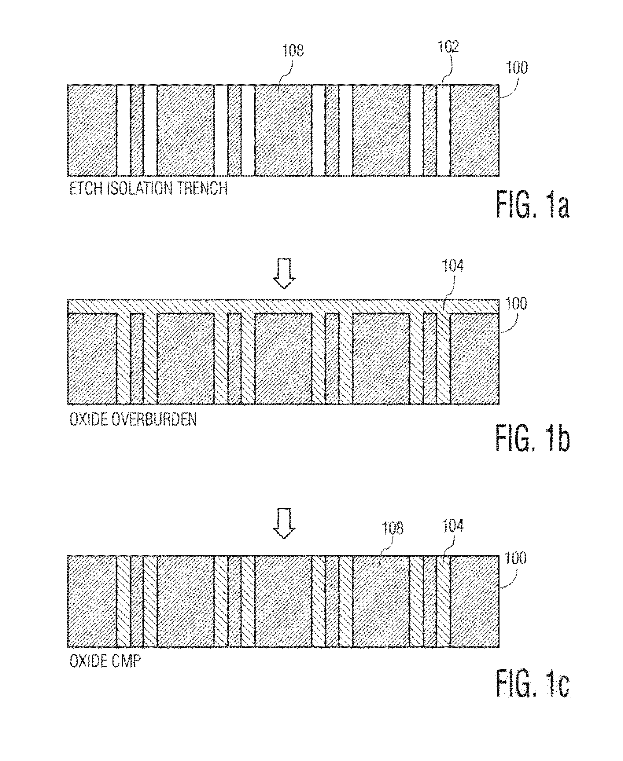
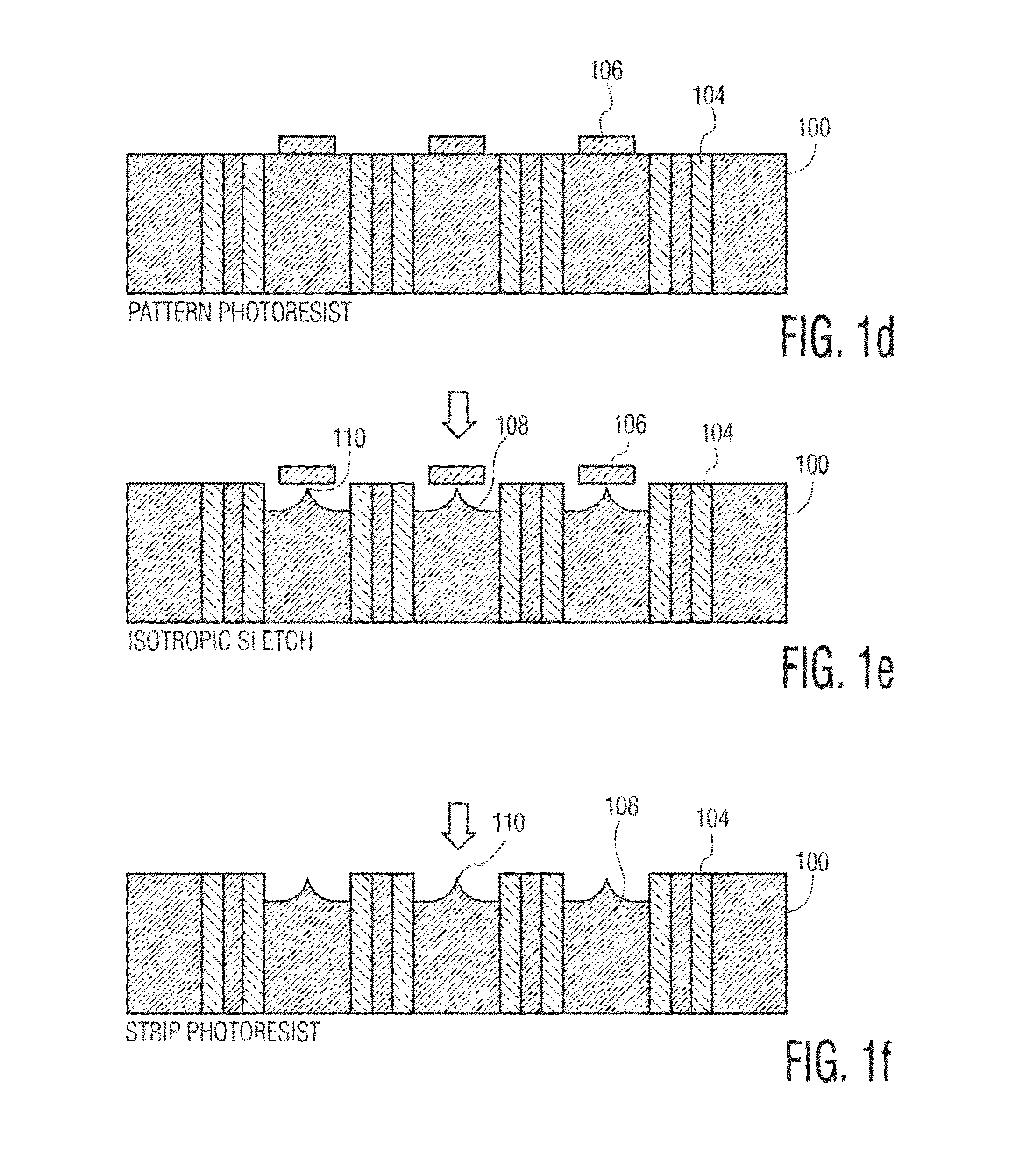
[0048]Field emission arrays have traditionally been fabricated using thin film deposition techniques (known as Spindt tips). The inventors have discovered that the use of micro-electromechanical systems (MEMS) processing technology to fabricate a field emission vacuum diode has beneficial effects.

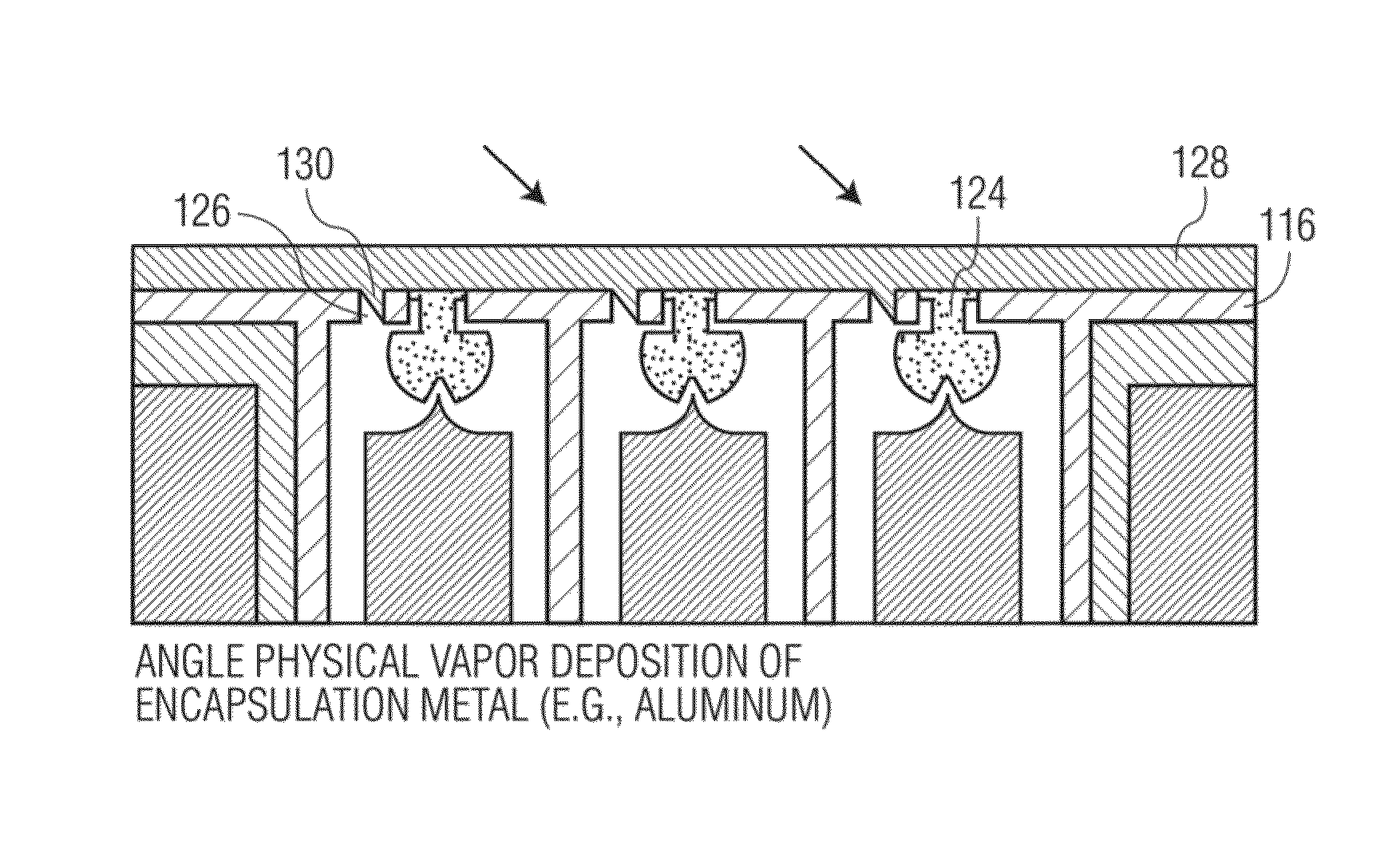
[0049]An exemplary device according to one aspect of the invention comprises an array of cold cathode field emitter tips, each associated with a blunt anode counter electrode. Both electrodes are in a vacuum cavity, created in-situ by physical vapor deposition of a metal film that seals the device at the deposition pressure, typically between 1E-03 and 1E-08 torr. An external vacuum chamber may also be incorporated to obtain sufficient vacuum levels.

[0050]When the exemplary device is forward biased, the field compression associated with the sharp tip of the cathode causes energy band bending that allows Fowler-Nordheim tunneling of electrons from the tip into vacuum, where they are attracte...


PUM


Abstract

Disclosed is an encapsulated micro-diode and a method for producing same. The method comprises forming a plurality columns in the substrate with a respective tip disposed at a first end of the column, the tip defining a cathode of the diode; disposing a sacrificial oxide layer on the substrate, plurality of columns and respective tips; forming respective trenches in the sacrificial oxide layer around the columns; forming an opening in the sacrificial oxide layer to expose a portion of the tips; depositing a conductive material in of the opening and on a surface of the substrate to form an anode of the diode; and removing the sacrificial oxide layer.

Description

STATEMENT REGARDING FEDERALLY SPONSORED RESEARCH[0001]This invention was developed under Contract DE-AC04-94AL85000 between Sandia Corporation and the U.S. Department of Energy. The U.S. Government has certain rights in this invention.FIELD OF THE INVENTION[0002]The present invention relates generally to field emission arrays. Specifically, the present invention relates to a cold cathode field emission vacuum diode.BACKGROUND OF THE INVENTION[0003]Conventionally, field emission arrays have been fabricated using thin film deposition techniques, also known as Spindt tips. Electrons emitted from the cathode (Spindt tip) are accelerated by the electric field between the cathode and the anode electrode. The cathode has an approximately conical shape, to which a predetermined electric field is applied so as to emit electrons. Moreover, when producing this Spindt type of electron emission device, a hole having a diameter of about 1 micrometer is formed and inside this hole, the emitter ele...

Claims


Application Information

Patent Timeline
IPC IPC(8): H01J9/04H01J3/02H01J9/02
CPCH01J3/022H01J9/025H01J19/32H01J19/54H01J1/36H01J19/46H01J21/20H01J19/24H01J1/3044H01J9/14H01J1/308
Inventor RESNICK, PAUL J.LANGLOIS, ERIC
Owner NAT TECH & ENG SOLUTIONS OF SANDIA LLC
Why Eureka
Try Eureka