

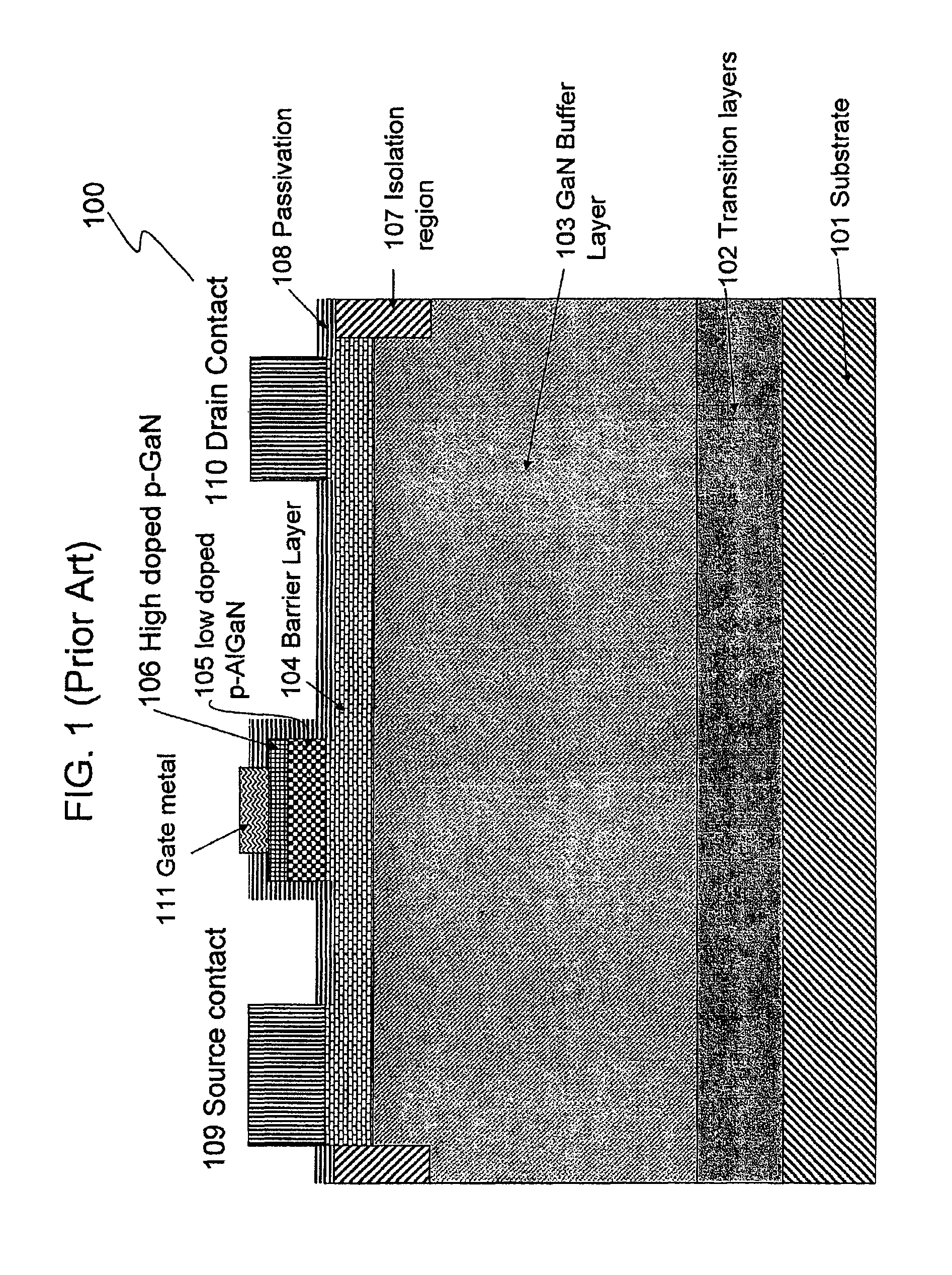
Enhancement mode GaN HEMT device with gate spacer and method for fabricating the same
a technology of enhanced mode and gate spacer, which is applied in the direction of semiconductor devices, basic electric elements, electrical equipment, etc., can solve the problems of high gate leakage current, high gate reliability risk, and increase manufacturing costs, so as to reduce manufacturing costs, reduce leakage, and reduce the effect of gate leakag
- Summary
- Abstract
- Description
- Claims
- Application Information
AI Technical Summary
Benefits of technology
Problems solved by technology
Method used
Image

Examples
first embodiment
[0021]Referring to FIGS. 2 and 3A-3H, a first embodiment is now described for forming an enhancement mode GaN HEMT device with a gate spacer and a self-aligned gate, wherein like reference numbers are used consistently for like features throughout the drawings.
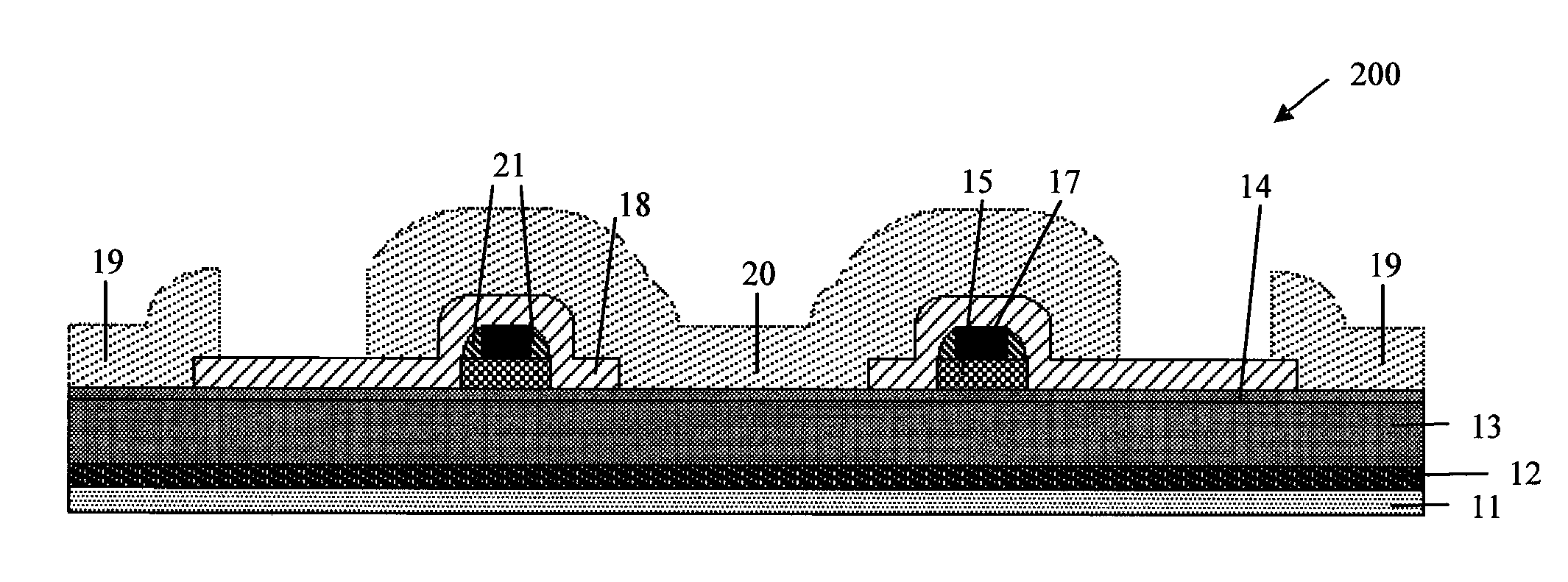
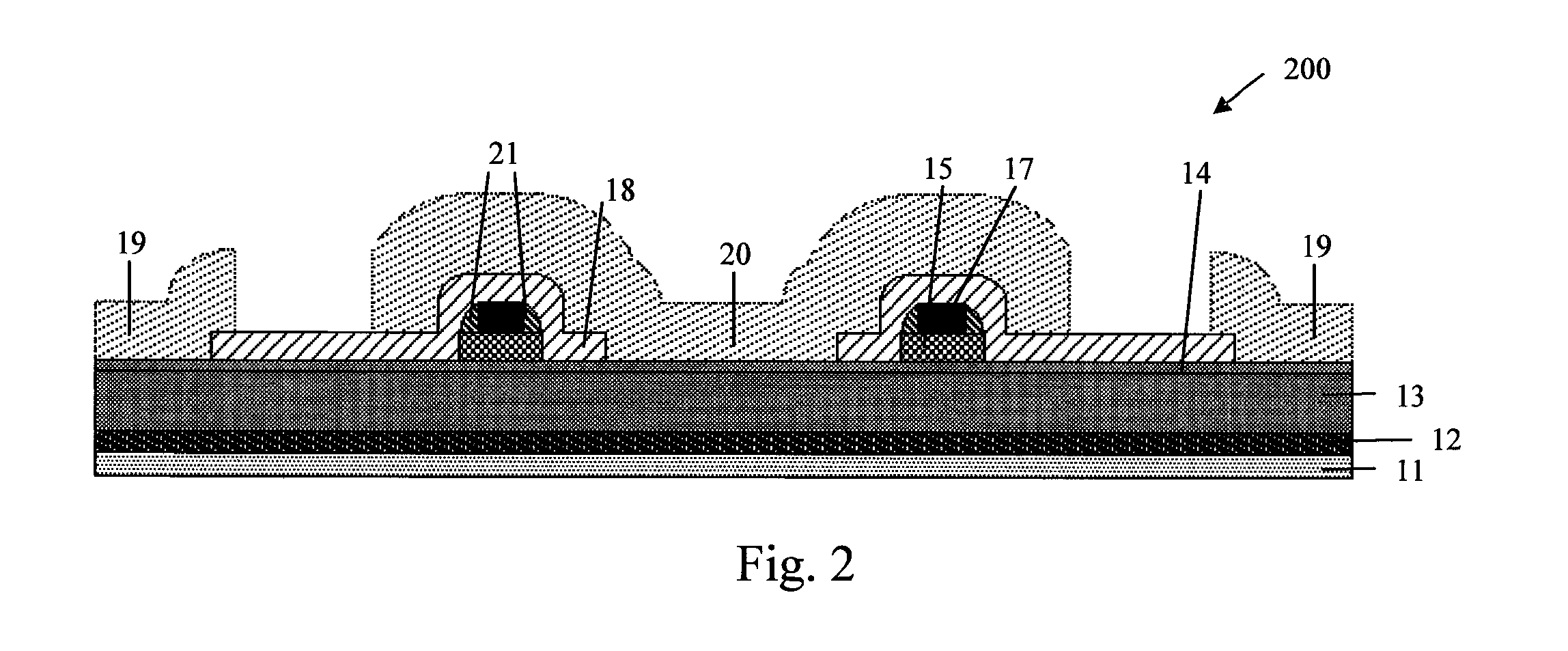
[0022]FIG. 2 illustrates an enhancement mode GaN HEMT device 200 formed by the method described below with respect to FIGS. 3A-3H, which has a gate metal 17 and III-V gate compound 15 that are self-aligned. Device 200 includes a silicon substrate 11, a buffer material 12, an un-doped GaN buffer material 13, an un-doped AlGaN barrier material 14, the III-V gate compound 15, the gate metal 17, a dielectric material 18, a drain ohmic contact 19, a source ohmic contact 20 and a dielectric spacer 21. The source metal 20 also serves as a field plate that extends over the gate and toward the drain contact.
[0023]FIG. 3A illustrates the EPI structure of the GaN HEMT device 200a, including, from bottom up, the silicon substrate 11, buff...
second embodiment
[0030]Referring to FIGS. 4 and 5A-5G, the invention is now described. FIG. 4 illustrates an enhancement mode GaN HEMT device 300 having a gate spacer 21 formed by the method shown in FIGS. 5A-5G. The resulting device 300 will have a gate metal 17 and gate compound 15 that are self-aligned. Device 300 in FIG. 4 differs from device 200 of FIG. 2 in that device 300 includes spacers 21 that are formed not only on the sidewalls of the gate metal 17, but also on the sidewalls of the III-V gate compound 15.
[0031]FIG. 5A illustrates the EPI structure 300a, including, from bottom to top, silicon substrate 11, buffer material 12, un-doped GaN buffer material 13, un-doped AlGaN barrier material 14, and the III-V gate compound material 15. The dimensions and compositions of the various materials are similar to that of the first embodiment.
[0032]As shown in FIG. 5B, as in the first embodiment, gate metal 17 is deposited or grown on the EPI structure shown in FIG. 5A.
[0033]Subsequently, a single ...
third embodiment
[0038]Referring now to FIGS. 6 and 7A-7H, the present invention is now described. FIG. 6 illustrates an enhancement mode GaN HEMT device 400 formed by the method described below with respect to FIGS. 7A-7H, which has a gate metal 17 and III-V gate compound 15 that are self-aligned. Device 400 includes a silicon substrate 11, a buffer material 12, an un-doped GaN buffer material 13, an un-doped AlGaN barrier material 14, the III-V gate compound 15, the gate metal 17, a dielectric material 18, a drain ohmic contact 19, a source ohmic contact 20, a dielectric spacer 21 and a dielectric film 22. The source metal 20 also serves as a field plate that extends over the gate and toward the drain contact.
[0039]FIG. 7A illustrates the EPI structure of the GaN HEMT device 400a, including, from bottom up, the silicon substrate 11, buffer material 12, un-doped GaN buffer material 13, un-doped AlGaN barrier material 14, and the III-V gate compound material 15. The un-doped GaN buffer material 13 p...
PUM
| Property | Measurement | Unit |
|---|---|---|
| thickness | aaaaa | aaaaa |
| dielectric | aaaaa | aaaaa |
| refractory | aaaaa | aaaaa |
Abstract
Description
Claims
Application Information