Organic electroluminescent devices

a technology of electroluminescent devices and organic materials, which is applied in the direction of organic semiconductor devices, solid-state devices, thermoelectric devices, etc., can solve the problems of failure of oled devices, unavoidable particle presence, dust for example, during the production process, etc., to prevent any damage to the electroluminescent layer stack, easy reproducible stress conditions, and reduce process costs

Active Publication Date: 2014-09-30
BEIJING XIAOMI MOBILE SOFTWARE CO LTD
View PDF12 Cites 0 Cited by
  • Summary
  • Abstract
  • Description
  • Claims
  • Application Information

AI Technical Summary

Benefits of technology

[0007]A counter electrode having tensile stress will increase the distance between the edges of a counter electrode and the substrate electrode around a defect in the electroluminescent layer (also denoted as layer defect), for example a hole defect caused by a dust particle present on top of the substrate electrode preventing material deposited in the neighborhood of the dust particle due to shadowing effect during layer deposition. However, a somehow upwards curved shape of the counter electrode adjacent to such a layer defect increasing the required field strength to initiate a short between counter and substrate electrode is suitable to lower the risk of shorts. To fully avoid the risk of shorts, the edges of the counter electrode have to be removed from the vicinity of a defect. A short prevention layer prepared on top of the counter electrode induces tensile stress to the layer system of counter electrode and short prevention layer. This enables the adjustment of the tensile stress of the double layer of counter electrode and the short prevention layer adhering to the counter electrode to be suitable to roll-up the double layer around a layer defect as a result of a weakened adhesion of the counter electrode on the organic electroluminescent layer stack around the layer defect. Here the term “roll-up” denotes the rolling-in or curling of the double layer analogue to a paper on a paper role. The roll-up of the double layer prevents shorts between counter electrode and substrate electrode due to the absence of the counter electrode adjacent to the defect. A flat counter electrode is still present as desired on non-disturbed organic electroluminescent layer(s). The term “double layer” shall denote a layer stack, where two essential components (counter electrode and short prevention layer) are present. The term “double layer” explicitly includes the possibility of additional layers between counter electrode and short prevention layer. Here the counter electrode shall be understood in a functional component to apply a voltage to the organic electroluminescent device. The counter electrode may be a layer or a layer stack of one or more layers required to establish a certain electrical conductivity to be able to act as an electrode. The short prevention layer shall be understood in a functional component to induce a certain tensile stress to the counter electrode, where the short prevention layer adheres to. The short prevention layer may be a layer or a layer stack of one or more layers required to induce a certain tensile stress.
[0029]The invention further relates to the use of a short prevention layer, preferably made of copper or manganese, in organic electroluminescent devices according to the present invention having a tensile stress suitable to roll-up a double layer of counter electrode and short prevention layer around a layer defect after partial dissolving the at least one organic electroluminescent layer arranged between substrate electrode and counter electrode in a vicinity of the defect to prevent shorts between the counter electrode and a substrate electrode before initial start-up of the organic electroluminescent devices. The use of the short prevention layer to prevent shorts is easily applicable to any kind of OLED devices and advantageous compared to alternative solutions Also shorts are prevented before operating the organic electroluminescent devices avoiding any leakage currents with layer defects subsequently avoiding any aging effects caused by these leakage currents.

Problems solved by technology

It is precisely in the case of large-area OLED layers covering a few square centimeters or more that the presence of particles, of dust for example, is unavoidable during the production process.
Particles present on the substrate, such for example as dust particles of a diameter substantially greater than the thickness of the electroluminescent layer stack, cause defects, e.g. holes in the adjacent electroluminescent layer stack with edges of an undefined nature.
These defects result in unacceptable leakage currents and short-circuits between the substrate electrode and counter electrode.
In contrast to a slow degradation of brightness due to the infiltration of oxygen or water into the light-emitting layers, failures of OLED devices as a result of short-circuits in the region of a defect become apparent as a sudden drop in brightness to zero.
It is precisely in the case of large-area OLED devices that short-circuits in the region of hole defects are by far the most common cause of failing OLED devices.
However, the remaining aluminum cathode layer around a hole defect still extend over the edges of the remaining organic layers around the hole defect and still has sharp edges of undefined nature.
If the electrically isolating layer does not fill the cavity underneath the aluminum cathode completely and subsequently isolate cathode from anode perfectly, there is still a risk of short-circuits.

Method used


Image

  • Organic electroluminescent devices
  • Organic electroluminescent devices

Examples


Embodiment Construction

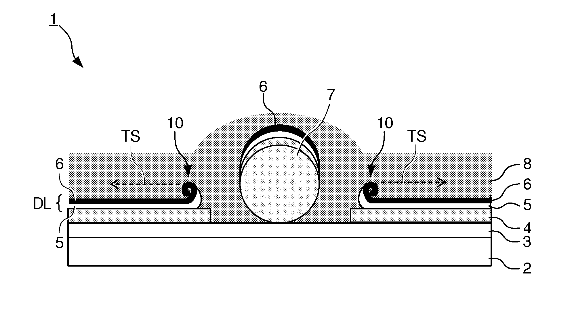
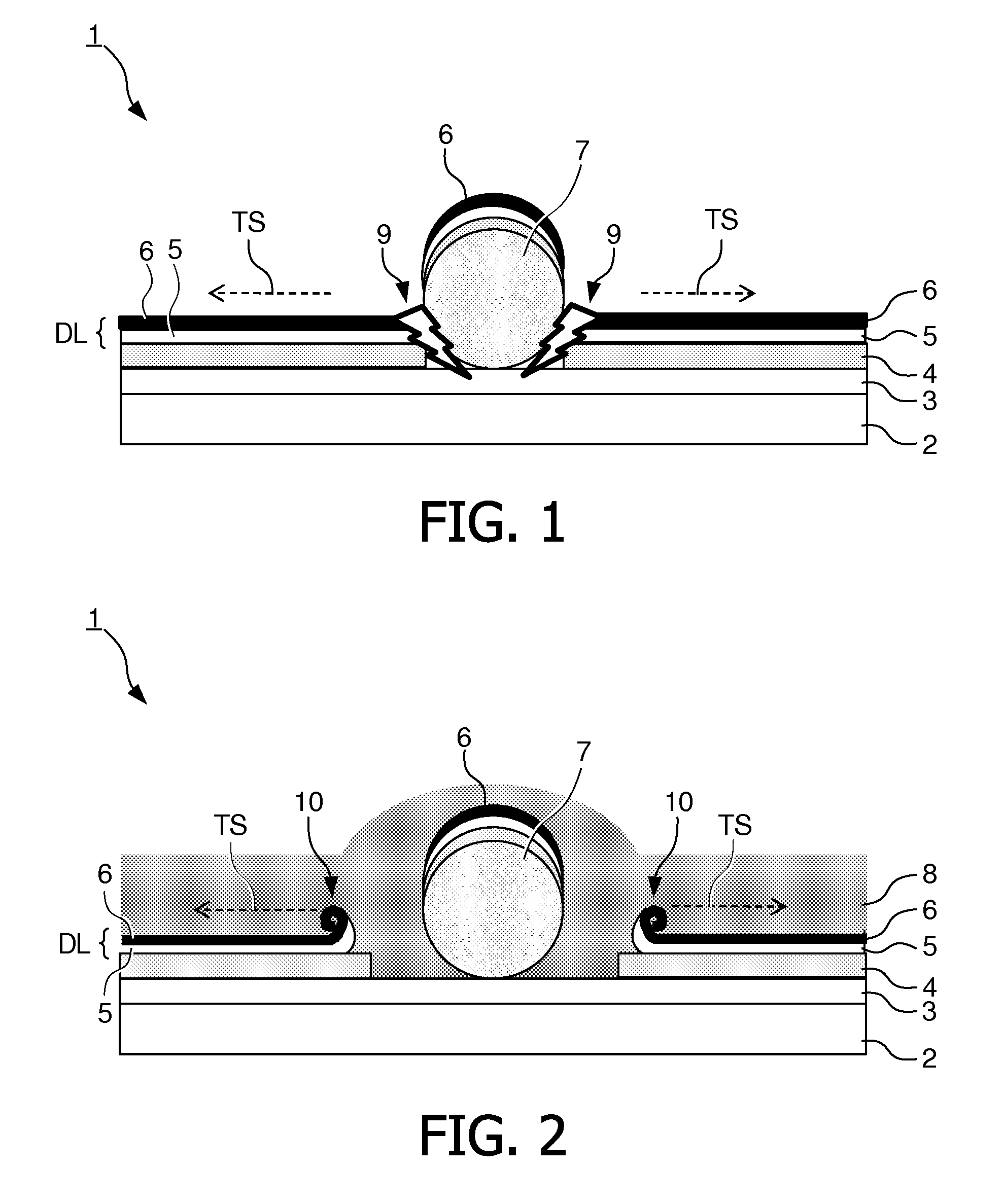
[0035]FIG. 1 is a schematic cross-sectional view of an OLED device 1 according to the present invention comprising a flat glass substrate 2 onto which a transparent ITO anode of a layer thickness of 120 nm as the substrate electrode 3 has been deposited by sputtering or CVD. On top of the substrate electrode 3 an organic electroluminescent layer stack 4 to emit light is deposited comprising a 25 nm thick hole injection layer of NHT-5 α-NPD doped with 4% F4-TCNQ, a 10 nm thick hole transport layer of α-NPD, a 30 nm thick organic light emitting layer of a matrix material with embedded light emitting small molecules, and a 50 nm thick electron transporting layer of TPBI. People skilled in the art may chose alternative electroluminescent layer stack with additional layers or with a lower number of layer or even with a single organic light emitting layer within the present invention. A counter electrode 5 made of aluminum with a thickness of 100 nm is evaporated on top of the organic ele...


PUM


Abstract

The invention relates to an organic electroluminescent device (1) comprising a substrate (2), at least one electroluminescent layer stack on top of the substrate (2) with at least a substrate electrode (3), a counter electrode (5) and at least one organic electroluminescent layer (4) arranged between substrate electrode (2) and counter electrode (5), and a short prevention layer (6) covering the counter electrode (5) establishing a double layer (DL) with a tensile stress (TS) induced by the short prevention layer (5), and an electrically isolating layer (8) at least partly covering the short prevention layer (6), wherein the electrically isolating layer (8) is suitable to partially dissolve the organic layer (4) in the vicinity of a defect (7) within the electroluminescent layer stack and the tensile stress (TS) induced by the short prevention layer (6) is suitable to roll up (10) the double layer (DL) adjacent to the defect (7) after deposition of the electrically isolating layer (8). The invention further relates to a method to manufacture such OLED devices (1) and the use of a short prevention layer (6) to prevent shorts in such OLED devices (1).

Description

FIELD OF THE INVENTION[0001]The invention relates to the field of organic electroluminescent devices (OLED devices) adapted to prevent shorts, a method to manufacture such OLEDs and the use of counter electrodes to prevent shorts in such OLED devices.BACKGROUND OF THE INVENTION[0002]Conventional organic electroluminescent (OLED) devices are usually produced by deposition of the electrodes and the required thin organic electroluminescent layer(s) on a transparent substrate such as glass or a polymer foil through which the light is emitted. When a voltage between around 2 and 10 Volts is applied between the two electrodes the electroluminescent layer or stack of layers emits light. In such OLED devices the electrode deposited onto the substrate—usually referred to as substrate electrode and also usually forming the anode—can be deposited as thin layer of an electrically conducting but optically transparent oxide, typically indium-tin oxide (ITO). The electrode opposing the substrate e...

Claims


Application Information

Patent Timeline
Patent Type & Authority Patents(United States)
IPC IPC(8): H01L33/00H01L21/00H01L51/00H01L35/24H01L31/12H01L29/26H01L29/08H01L29/16H01L27/15H01L51/52H01L51/56
CPCH01L51/5237H01L51/56H01L2251/5361H10K50/841H10K71/00H10K50/11H10K50/13H10K50/84H10K2102/302
Inventor BOERNER, HERBERT, F.
Owner BEIJING XIAOMI MOBILE SOFTWARE CO LTD
Why Eureka
Try Eureka