

Light emitting diode with metal piles and multi-passivation layers and its manufacturing method
a technology of light-emitting diodes and metal piles, which is applied in the manufacturing of semiconductor/solid-state devices, semiconductor devices, electrical devices, etc., can solve the problems of reducing the efficiency of reflector layers, and affecting the efficiency of semiconductor light-emitting diodes. , to achieve the effect of reducing the number of pads, preventing light absorption of pads, and enhancing optical power
- Summary
- Abstract
- Description
- Claims
- Application Information
AI Technical Summary
Benefits of technology
Problems solved by technology
Method used
Image

Examples
Embodiment Construction
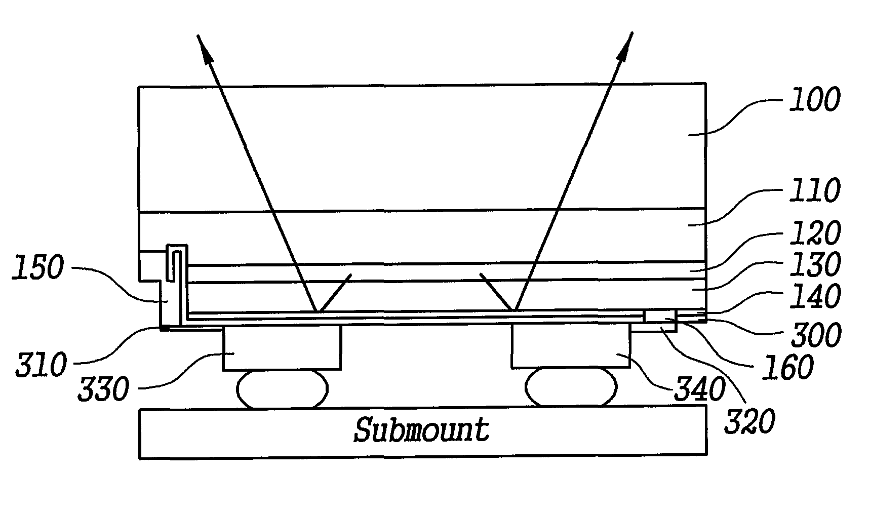
[0120]FIG. 9 is a cross-sectional view of a light emitting diode with pad rearrangement according to an embodiment of the present invention.
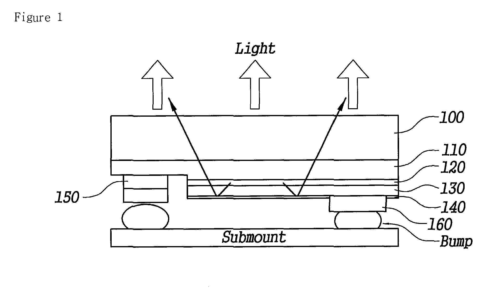
[0121]FIG. 9 shows a substrate 100, a first semiconductor layer 110, an active layer 120, a second semiconductor layer 130, a reflector layer 140, a first electrode 150, a second electrode 160, a first passivation layer 300, a first electrode line 310, a second electrode line 320, a first bonding pad 330, and a second bonding pad 340 (see FIG. 19).
[0122]The first semiconductor layer 110 and the second semiconductor layer 130 are made of GaN, and the layers are stacked on the substrate 100.
[0123]The active layer 120 is formed between the first semiconductor layer 110 and the second semiconductor layer 130.
[0124]The reflector layer 140 is formed on a part of stacked semiconductor layers which are formed of a first semiconductor layer 110, an active layer 120, and a second semiconductor layer 130 in sequence, except the lowered face prepared with m...
PUM
 Abstract
Description
Claims
Application Information