Devices and methods for solder flow control in three-dimensional microstructures

a three-dimensional microstructure and flow control technology, applied in the direction of sustainable manufacturing/processing, semiconductor/solid-state device details, cable terminations, etc., can solve the problems of void spaces, void spaces, and different surface height changes,

Inactive Publication Date: 2014-10-21
CUBIC CORPORATION
View PDF178 Cites 15 Cited by
  • Summary
  • Abstract
  • Description
  • Claims
  • Application Information

AI Technical Summary

Benefits of technology

[0008]In one of its aspects, the present invention provides exemplary devices and methods in which mechanical interlocking the of the layers by overlapping their boundaries in three-dimensional cross-section provides mechanical and positional stability despite the large change in temperature associated with reflowing a material such as solder would induce, which can be on the order of 200° C. or more. In this regard, the present invention provides devices and methods in which reliance on chemical adhesion alone to keep the materials intact is not required.

Problems solved by technology

With increasing demands on computational power and data transmission bandwidth, electronic devices and microstructures incorporating such devices are becoming increasingly complex necessitating a greater degree of mechanical and electrical interconnection among components.
However, it may be difficult to stop solder from wicking up the length of a metal component, especially in view of the complex surface morphologies which may be encountered in three-dimensional microstructures, and particularly when such structures are made of or coated with metals such as gold, silver, copper or similar metals which are capable of promoting solder flow.
For instance, the presence of a multitude of discrete components, mounting surfaces, interconnected chips, and so on presents a variety of surface height changes and void spaces prone to wicking molten solder along the surfaces of such components.
A clean thin layer of gold on platinum, intended for solder reflow, may for example, continue to wet the surface particularly in non-oxidizing conditions for a great distance until the solder thickness or composition due to interdiffusion becomes unacceptable for its intended purpose.
The unintended flow of solder throughout such microstructures may cause decreased performance, uncontrolled bond lines, shorting, solder embrittlement, and other problems.
Whereas a “solder mask”, such as a patterned planar dielectric coating, may be used to stop and / or control solder flow, in an open three-dimensional structure applying such a material may be relatively difficult to achieve for multiple reasons.
Second, a complex three-dimensional structure may be hard to coat and / or pattern lithographically on more than one layer.
Third, it may be desirable to ensure substantially complete removal of any existing solder mask materials as they may degrade performance such as RF performance, because they may not be applied with sufficient accuracy and / or quantity for many applications (e.g., microwave devices) onto such three-dimensional structures.
These problems are aggravated when the desired pad dimensions for a solder or conductive adhesive continue to shrink from squares of hundreds of microns on a side to squares of tens of microns, as currently is the case for some microwave and mm-wave devices and circuits such as MMICs.
In addition, three-dimensional microstructures may include coatings of excellent conductors and / or noble metals, such as gold, which may aggravate a problem of solder flowing along a conductor in an uncontrolled manner.
Previous approaches for three-dimensional microstructures have failed to disclose how to maintain adhesion of such coatings particularly when the CTE match of the wettable metals and the non-wettable layers or “wick stop” materials may be highly mismatched.

Method used


Image

  • Devices and methods for solder flow control in three-dimensional microstructures
  • Devices and methods for solder flow control in three-dimensional microstructures
  • Devices and methods for solder flow control in three-dimensional microstructures

Examples


Embodiment Construction

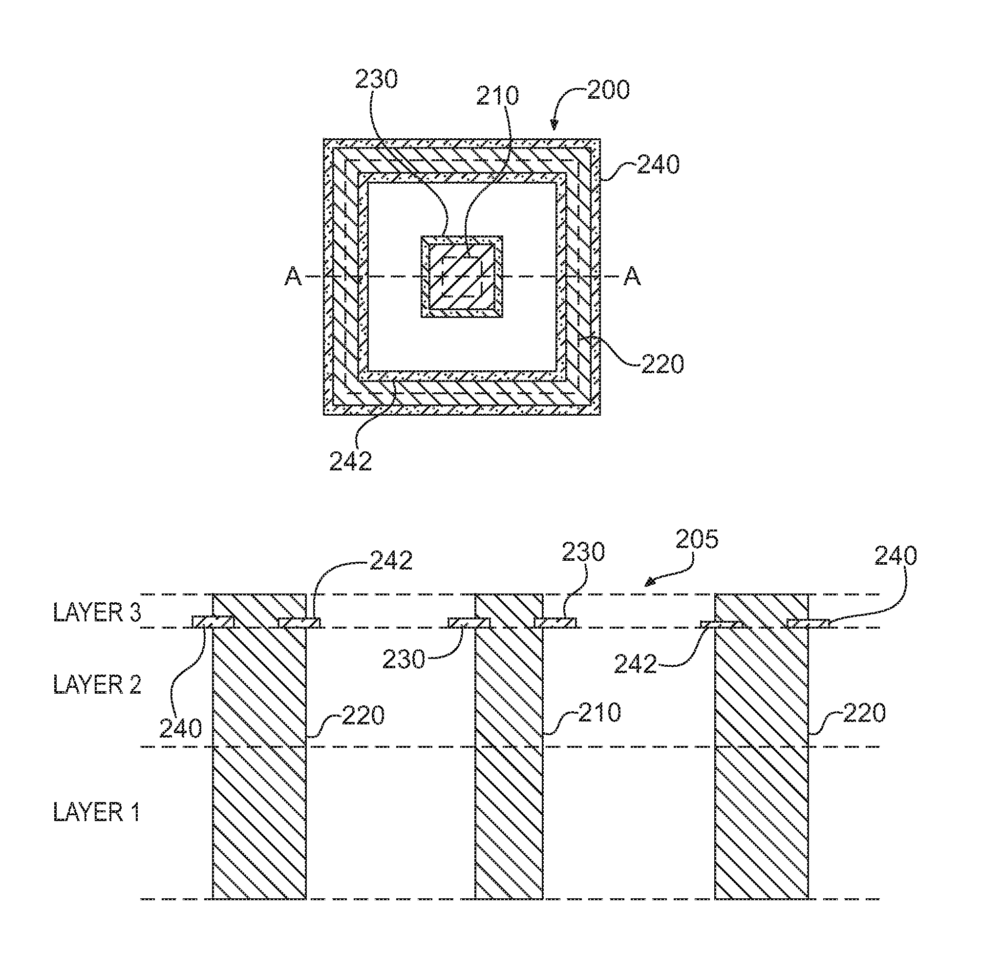
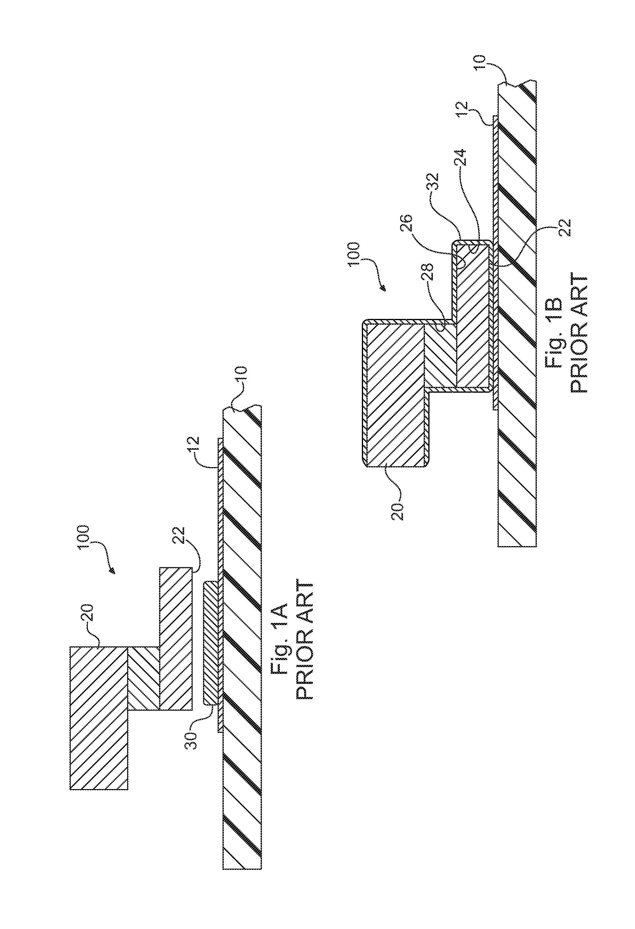
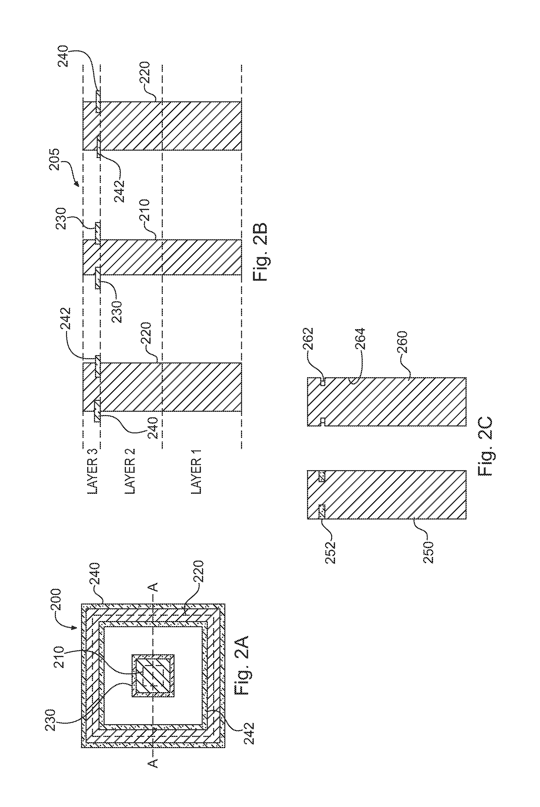
[0024]Referring now to the figures, wherein like elements are numbered alike throughout, an aspect of the present invention may be understood by reference to FIGS. 1A-1B in which one of the problems addressed by the present invention is illustrated. FIG. 1A schematically illustrates a device 100 prior to assembly comprising a portion of a three-dimensional microstructure 20 for electrical and / or mechanical connection to a base layer 10, such as a circuit board. The base layer 10 may include a metal component, such as a circuit board trace 12, to which the three-dimensional microstructure 20 is to be attached, and attachment may be effected through the use of a solder 30 disposed between a mounting surface 22 of the three-dimensional microstructure 20 and the circuit board trace 12. The microstructure may for example be comprised of copper with a thin surface coating of nickel and gold as is common for an electrical conductor in microelectronics. Upon heating, the solder 30 is melted...


PUM

PropertyMeasurementUnit
temperatureaaaaaaaaaa
heightaaaaaaaaaa
electronic microstructureaaaaaaaaaa

Abstract

Structures, materials, and methods to control the spread of a solder material or other flowable conductive material in electronic and/or electromagnetic devices are provided.

Description

RELATED APPLICATIONS[0001]This application claims the benefit of priority of U.S. Provisional Application No. 61 / 493,516, filed on Jun. 5, 2011, the entire contents of which application are incorporated herein by reference.FIELD OF THE INVENTION[0002]The present invention relates generally to control of the flow of a conductive material in electric, electronic and / or electromagnetic devices, such as three-dimensional microstructures (e.g., waveguide structures), and more particularly, but not exclusively, to structures, materials, and methods to control the spread of a solder material or other flowable conductive material, such as a conductive epoxy.BACKGROUND OF THE INVENTION[0003]With increasing demands on computational power and data transmission bandwidth, electronic devices and microstructures incorporating such devices are becoming increasingly complex necessitating a greater degree of mechanical and electrical interconnection among components. In response, three-dimensional m...

Claims


Application Information

Patent Timeline
Patent Type & Authority Patents(United States)
IPC IPC(8): H02G15/00H01L23/48
CPCB81C1/00357B81C2201/019H01L24/83H01L2224/26175H01L2224/3015H01L2224/32227H01L2224/83191H01L2224/83815H05K3/34H05K3/321H05K3/4007H05K2201/10787H05K2201/10984H05K2203/0465H05K2203/1173H01L2924/12042H01L2224/291H05K1/111Y02P70/50H01L2924/00014H01L2924/00H01L2924/014H01L24/26H05K1/181H05K3/341H05K2201/10674
Inventor SHERRER, DAVID W.REID, JR., JAMES R.
Owner CUBIC CORPORATION
Why Eureka
Try Eureka