Organic EL element

a light-emitting element and organic technology, applied in the field of organic electricfield light-emitting elements, can solve the problems of increasing the difficulty increasing the difficulty of application, and increasing the difficulty of maintaining the precision of mask position adjustment, so as to reduce the barrier of hole injection, high hole injection efficiency, and low voltage

Active Publication Date: 2014-11-11
JOLED INC
View PDF136 Cites 9 Cited by
  • Summary
  • Abstract
  • Description
  • Claims
  • Application Information

AI Technical Summary

Benefits of technology

[0028]According to the organic EL element that is one aspect of the present invention, the hole injection layer comprises tungsten oxide, and is at least 2 nm thick. The hole injection layer includes an occupied energy level that is 1.8 electron volts to 3.6 electron volts lower than a lowest energy level of a valence band of the hole injection layer in terms of a binding energy. According to the organic EL element that is one aspect of the present invention, with use of the occupied energy level of the hole injection layer, it is possible to extremely reduce the hole injection barrier between the Fermi level of the anode and the occupied energy level of the hole injection layer and the hole injection barrier between the occupied energy level of the hole injection layer and the highest occupied molecular orbital (HOMO) of the functional layer. As a result, the organic EL element that is one aspect of the present invention achieves high hole injection efficiency, and realizes driving at a low voltage and promises excellent light-emitting efficiency due to the high hole injection efficiency.
[0029]Also, according to the organic EL element that is one aspect of the present invention, with no special strict adjustment or maintenance of the surface conditions of the anode, it is possible to stably reduce the hole injection barrier between the anode and the hole injection layer during normal manufacturing process. Accordingly, manufacturing of organic EL elements having stable performance requires no high control on the surface conditions of the anode. Therefore, the organic EL element that is one aspect of the present invention facilitates manufacturing of large-sized organic EL panels at comparatively low costs, and is excellent in feasibility.

Problems solved by technology

However, although vapor deposition-type organic EL elements may be ideal for use in small-sized organic EL panels, application thereof is extremely difficult, for example, to full-color, large-sized organic EL panels having display sizes of around 100 inches.
The difficulty of such an application derives from the technology applied in the manufacturing of a vapor deposition-type organic EL element.
However, as the surface area of the organic EL panel to be manufactured becomes larger, it becomes more and more difficult to maintain the precision with which mask position adjustment is performed.
Hence, the manufacturing of a large-sized display without any deficiencies is extremely difficult when applying vapor deposition-type organic EL elements.

Method used


Image

  • Organic EL element
  • Organic EL element
  • Organic EL element

Examples


embodiment 1

(Structure of Organic EL Element)

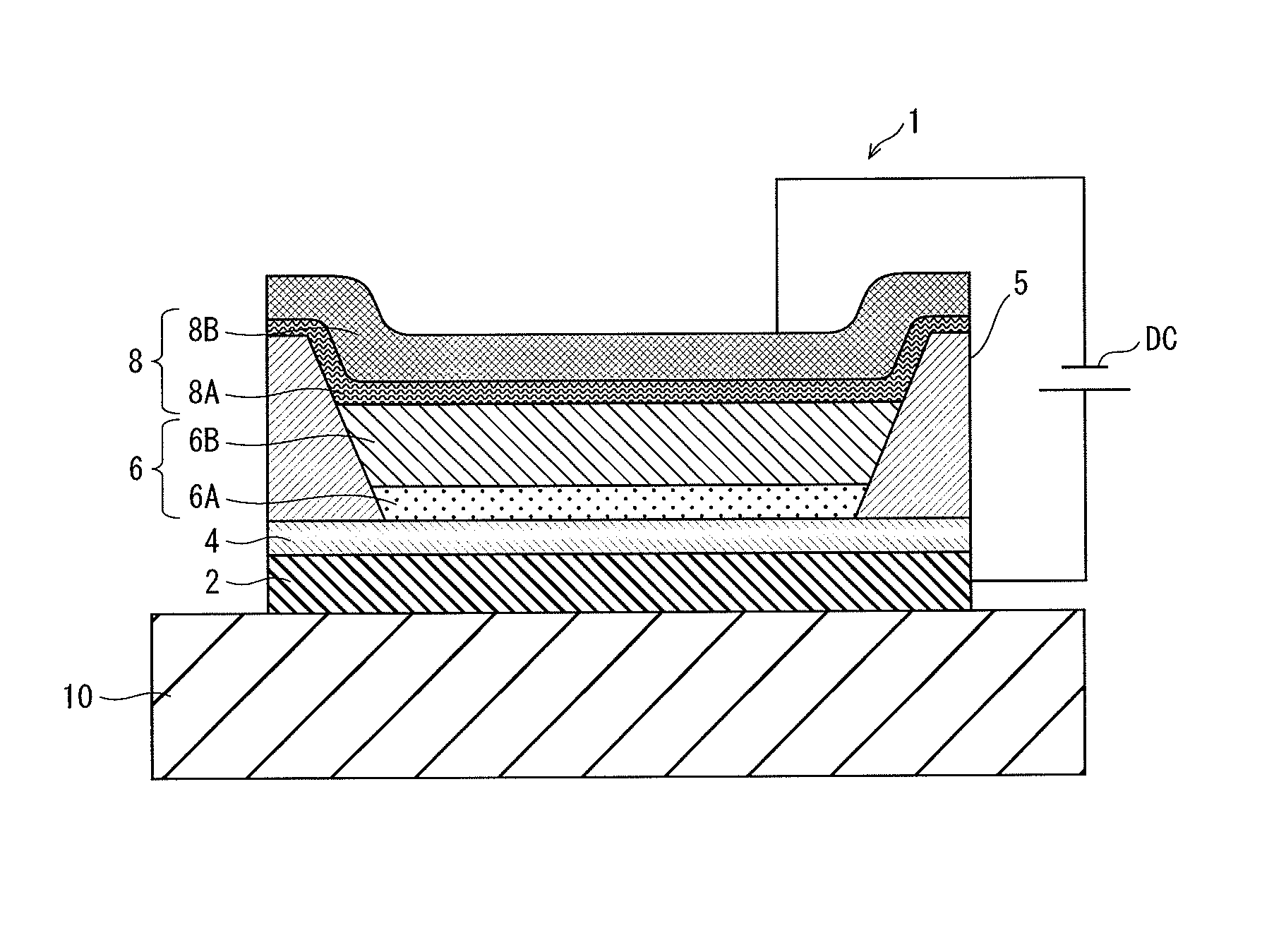
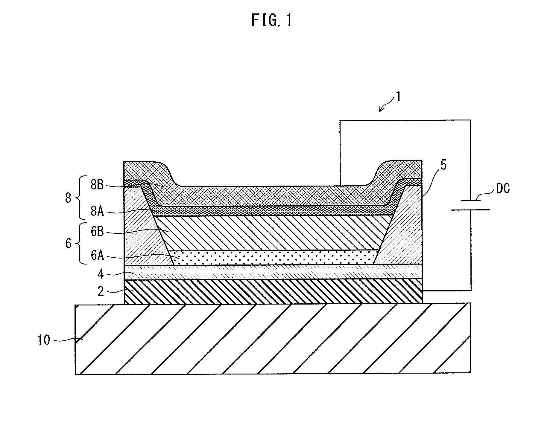
[0113]FIG. 1 is a schematic cross-sectional view illustrating the structure of an organic EL element 1 pertaining to Embodiment 1.

[0114]The organic EL element 1 is an application-type organic EL element, which is characterized in that a functional layer is applied by a wet process in the manufacturing thereof. The organic EL element 1 includes: a hole injection layer 4; various functional layers (a buffer layer 6A and a light-emitting layer 6B, in this case); and a pair of electrodes composed of an anode 2 and a cathode 8. The hole injection layer 4 and the functional layers are disposed one on top of the other, and are disposed between the pair of electrodes. Each of the functional layers contains functional material having a predetermined function.

[0115]More specifically, the organic EL element 1 includes, as illustrated in FIG. 1, the anode 2, the hole injection layer 4, the buffer layer 6A, the light-emitting layer 6B, and the cathode 8 (composed...

embodiment 2

1C>

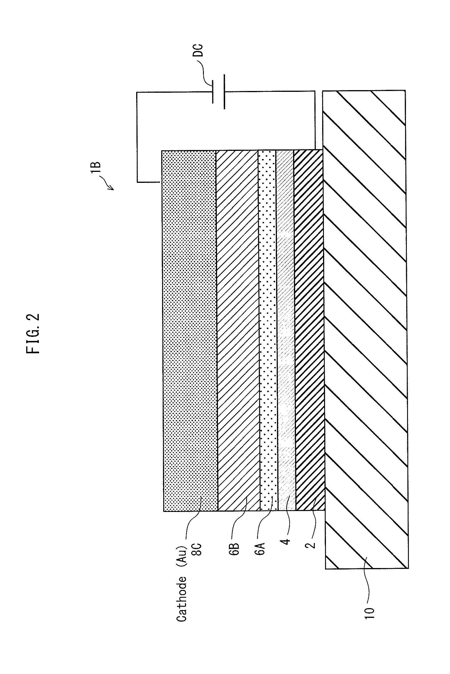
[0305]FIG. 25A is a schematic cross-sectional view illustrating the structure of an organic EL element 1C according to the present embodiment. FIG. 25B is a partially enlarged view illustrating the vicinity of a hole injection layer 4A.

[0306]The organic EL element 1C is for example an applying-type organic EL element, which is characterized in that a functional layer is applied by a wet process in the manufacturing thereof. The organic EL element 1 includes: a hole injection layer 4A; various functional layers; and a pair of electrodes composed of an anode 2 and a cathode 8D. The hole injection layer 4A and the functional layers are disposed one on top of the other, and are disposed between the pair of electrodes. Each of the functional layers contains functional material having a predetermined function.

[0307]More specifically, the organic EL element 1C includes the anode 2, an ITO layer 3, the hole injection layer 4A, a buffer layer 6A, a light-emitting layer 6B, an electron inj...


PUM


Abstract

Provided is an organic EL element which withstands mass production of organic EL display panels, and promises driving at a low voltage and high luminous efficiency due to excellent hole-injection efficiency. Specifically, an organic EL element is formed by sequentially laminating an anode, a hole injection layer, a buffer layer, a light-emitting layer, and a cathode on one surface of a substrate. The hole injection layer is a at least 2 nm thick tungsten oxide layer formed under predetermined film forming conditions, and includes an occupied energy level that is 1.8 eV to 3.6 eV lower than a lowest energy level of a valence band of the hole injection layer in terms of a binding energy. This reduces the hole injection barrier between the anode and the hole injection layer and the hole injection barrier between the hole injection layer and the buffer layer.

Description

TECHNICAL FIELD[0001]The present invention relates to an organic electric-field light-emitting element (referred to hereinafter as an “organic EL element”), which is an electric light emitter. Particularly, the present invention relates to a technology for driving such an organic EL element at low electricity while ensuring a wide range of luminous intensity from low luminous intensity to high luminous intensity for the use as a light source or the like.BACKGROUND ART[0002]In recent years, progress is being made in research and development of diverse functional elements which involve the use of an organic semiconductor.[0003]Organic EL elements are known as being one of the most common among such functional elements. An organic EL element is an electric current-driven light emitter, and commonly includes a pair of electrodes consisting of an anode and a cathode, and a functional layer containing organic material disposed between the pair of electrodes. The functional layer includes ...

Claims


Application Information

Patent Timeline
Patent Type & Authority Patents(United States)
IPC IPC(8): H01L51/56H01L51/50H01L29/08H01L51/52
CPCH01L51/56H01L51/52H01L51/5088H01L2251/55H10K50/17H10K2101/00H10K50/80H10K71/00
Inventor OHUCHI, SATORUYAMADA, RYUUTAKOMATSU, TAKAHIROFUJIMURA, SHINYAFUJITA, HIROFUMINENDAI, KENICHISUGANO, KOUYADA, SHUHEI
Owner JOLED INC
Why Eureka
Try Eureka