Block structure profiling in three dimensional memory

a three-dimensional memory and block structure technology, applied in the direction of digital storage, instruments, semiconductor devices, etc., can solve the problems of non-uniformity of memory holes along their length, earlier failure, etc., and achieve the effect of light us

Active Publication Date: 2014-12-02
SANDISK TECH LLC
View PDF45 Cites 25 Cited by
  • Summary
  • Abstract
  • Description
  • Claims
  • Application Information

AI Technical Summary

Benefits of technology

[0007]In some 3-D memory arrays, characteristics of a memory cell may depend on the diameter of a memory hole where it intersects the memory cell. Memory holes may be non-uniform along their length, and different memory holes may have different profiles. Memory hole diameter may be calculated from characteristics that are observed during programming. Knowing a memory hole profile of a block allows suitable operating parameters to be selected for operating the block. Memory hole profile of a plane may be used to select operating parameters for the plane. Memory hole profile of a die may be used to select operating parameters for the die. Smaller memory holes result in earlier failure. Hot counts may be adjusted according to memory hole size so that blocks that are expected to fail earlier because of small memory holes are more lightly used than blocks with larger memory holes.

Problems solved by technology

Memory holes may be non-uniform along their length, and different memory holes may have different profiles.
Smaller memory holes result in earlier failure.

Method used


Image

  • Block structure profiling in three dimensional memory
  • Block structure profiling in three dimensional memory
  • Block structure profiling in three dimensional memory

Examples


Embodiment Construction
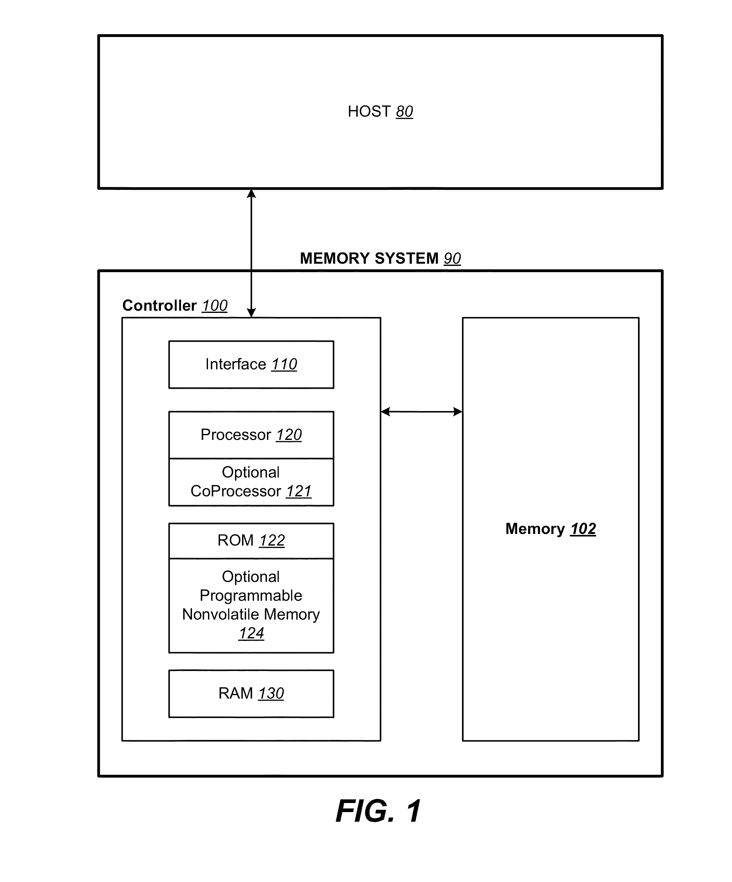
Memory System

[0036]FIG. 1 illustrates schematically the main hardware components of a memory system suitable for implementing the present invention. The memory system 90 typically operates with a host 80 through a host interface. The memory system may be in the form of a removable memory such as a memory card, or may be in the form of an embedded memory system. The memory system 90 includes a memory 102 whose operations are controlled by a controller 100. The memory 102 comprises one or more array of non-volatile memory cells distributed over one or more integrated circuit chip. The controller 100 may include interface circuits 110, a processor 120, ROM (read-only-memory) 122, RAM (random access memory) 130, programmable nonvolatile memory 124, and additional components. The controller is typically formed as an ASIC (application specific integrated circuit) and the components included in such an ASIC generally depend on the particular application.

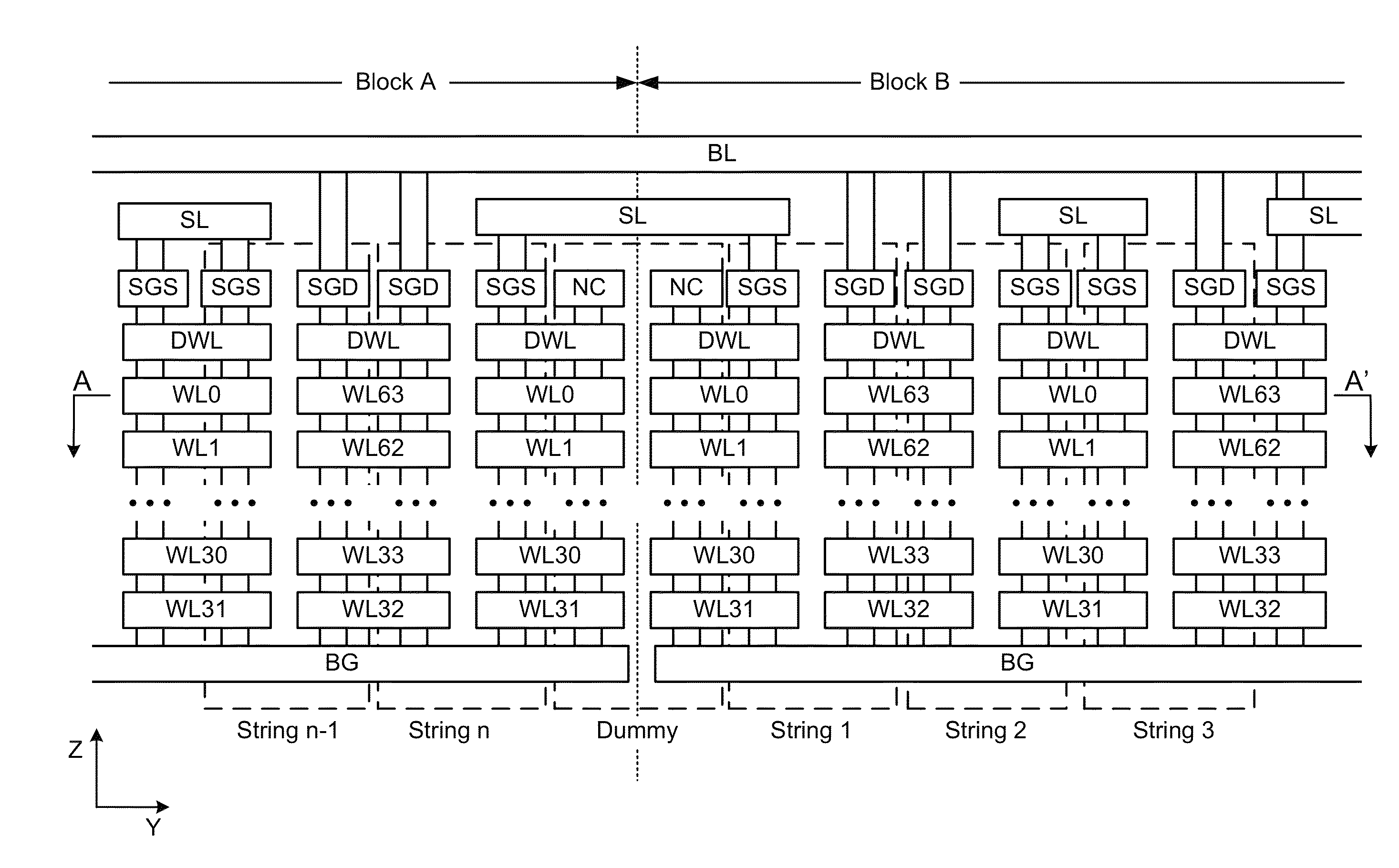
Physical Memory Structure

[0037]FIG. ...


PUM


Abstract

Memory hole diameter in a three dimensional memory array may be calculated from characteristics that are observed during programming. Suitable operating parameters may be selected for operating a block based on memory hole diameters. Hot counts of blocks may be adjusted according to memory hole size so that blocks that are expected to fail earlier because of small memory holes are more lightly used than blocks with larger memory holes.

Description

CROSS-RELATED APPLICATION[0001]This application is a continuation of U.S. application Ser. No. 14 / 064,823 filed Oct. 28, 2013, which application is incorporated herein in its entirety by this reference.BACKGROUND[0002]This application relates to the operation of re-programmable nonvolatile three dimensional memory systems such as semiconductor flash memory which record data using charge stored in charge storage elements of memory cells.[0003]Solid-state memory capable of nonvolatile storage of charge, particularly in the form of EEPROM and flash EEPROM packaged as a small form factor card, has become the storage of choice in a variety of mobile and handheld devices, notably information appliances and consumer electronics products. Unlike RAM (random access memory) that is also solid-state memory, flash memory is non-volatile, and retains its stored data even after power is turned off, Also, unlike ROM (read only memory), flash memory is rewritable similar to a disk storage device. I...

Claims


Application Information

Patent Timeline
Patent Type & Authority Patents(United States)
IPC IPC(8): G11C16/26H01L27/115G11C16/10G11C16/04G11C29/00
CPCG11C29/00G11C16/26H01L27/115G11C16/10G11C16/0483G11C29/08G11C11/5628G11C11/5642G11C29/021G11C29/028H01L27/1157H01L27/11582H10B43/35H10B43/27H10B69/00
Inventor RAGHU, DEEPAKDUSIJA, GAUTAM A.AVILA, CHRISDONG, YINGDAMUI, MANMAK, ALEXANDER KWOK-TUNGKOH, PAO-LING
Owner SANDISK TECH LLC
Why Eureka
Try Eureka