Semiconductor structure

a technology of semiconductors and structures, applied in the direction of semiconductor devices, resistors, electrical equipment, etc., can solve the problems of reducing competitiveness in the market and increasing process costs, and achieve the effect of easy formation

Active Publication Date: 2014-12-09
POWERCHIP SEMICON MFG CORP
View PDF12 Cites 6 Cited by
  • Summary
  • Abstract
  • Description
  • Claims
  • Application Information

AI Technical Summary

Benefits of technology

[0008]Accordingly, the present invention provides a method of forming a semiconductor structure. The semiconductor structure including a memory unit and a resistor can be easily formed with the existing process, and the formed structure meet the customers' electrical requirements.
[0024]In view of the above, the manufacturing method of the present invention can be easily integrated with the existing process (e.g. logic process). The semiconductor structure including a memory unit and a resistor can be easily formed with the existing process, so that the process cost is greatly reduced, and the competitive advantage is achieved. The said memory unit can be an ETOX structure or a two-transistor (2T) structure including a charge storage structure and a select gate, and is capable of one-time programming (OTP) or multiple-time programming (MTP) operation according to the customers' requirements.

Problems solved by technology

Therefore, multiple photomasks and complicated process steps are required, so as to increase the process cost and reduce the competitiveness in the market.

Method used


Image

  • Semiconductor structure
  • Semiconductor structure
  • Semiconductor structure

Examples


first embodiment

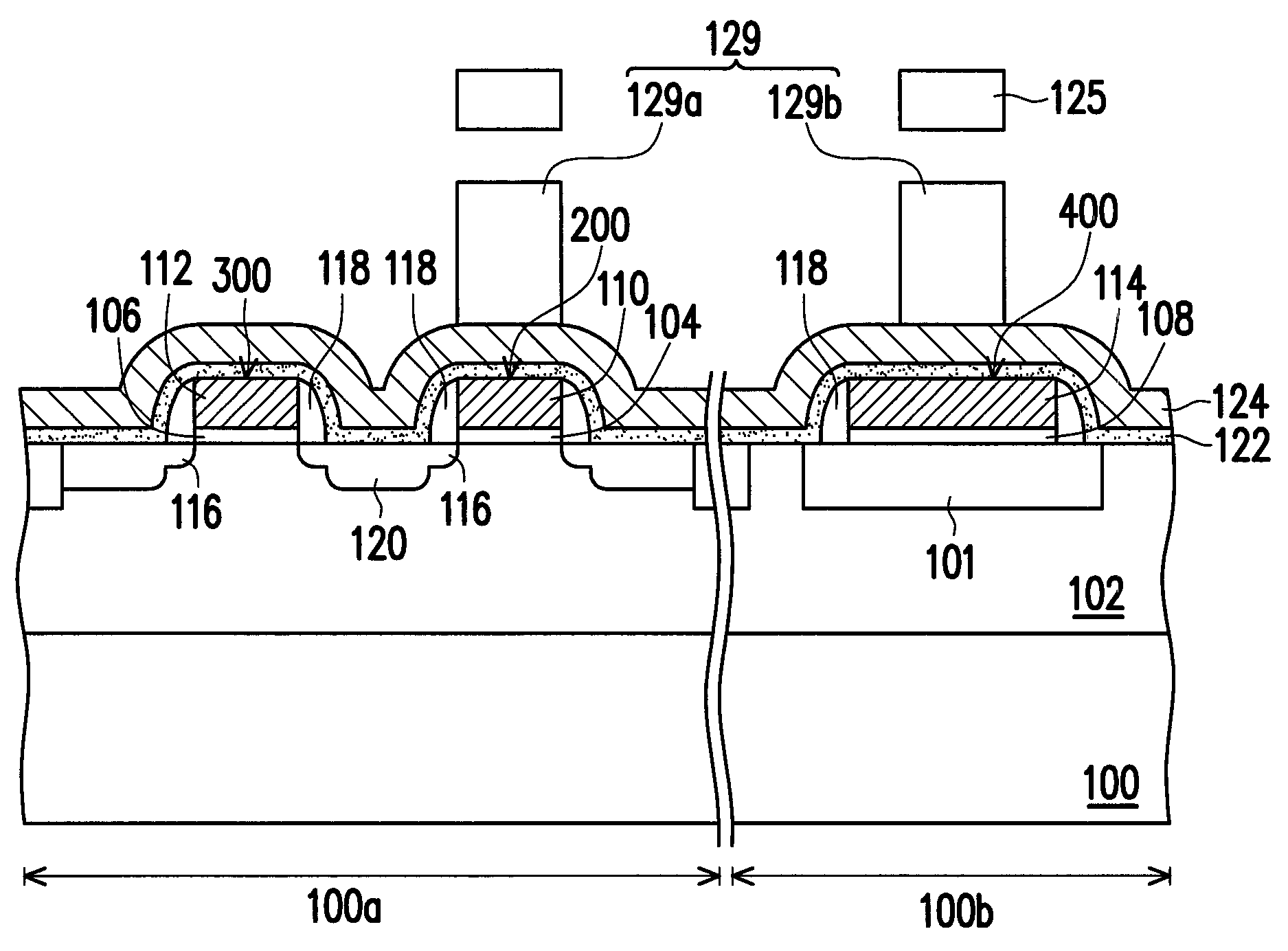
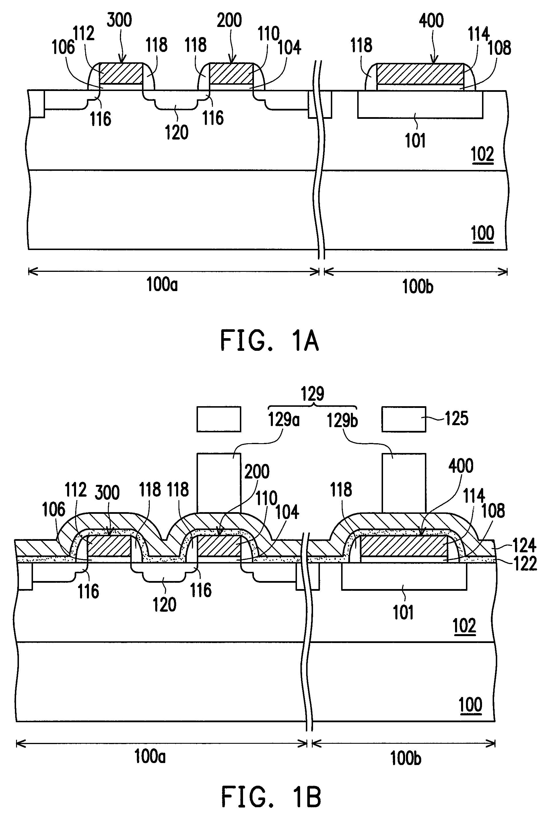
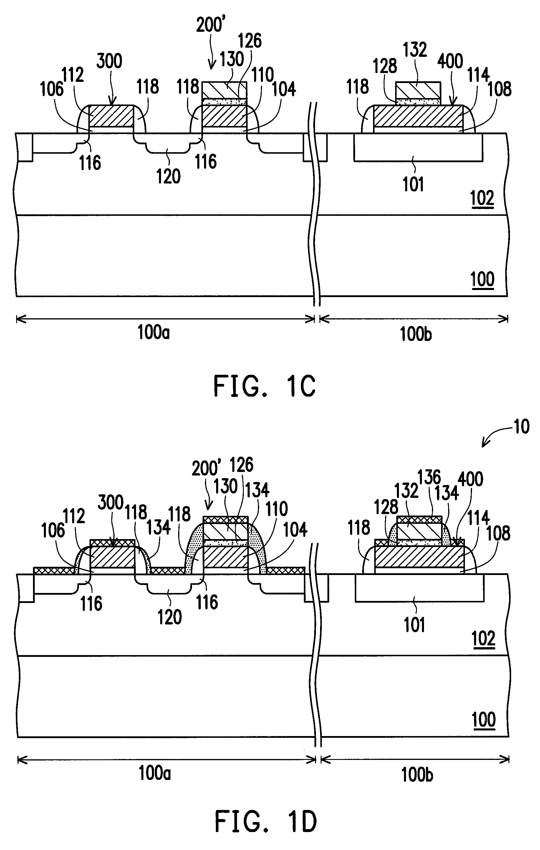
[0030]FIGS. 1A to 1D schematically illustrate cross-sectional views of a method of forming a semiconductor structure according to a first embodiment of the present invention.

[0031]Referring to FIG. 1A, a substrate 100 is provided. The substrate 100 is a P-type silicon substrate, for example. The substrate 100 has a cell area 100a and a periphery area 100b. A well region 102 is formed in the substrate 100. The well region 102 is a P-type well region, for example. In an embodiment, a deep well region (not shown) can be optionally formed in the substrate 100 below the well region 102. Further, a plurality of shallow trench isolation (STI) structures 101 is formed in the substrate 100, and at least one STI structures 101 is located in the substrate 100 in the periphery area 100b.

[0032]Thereafter, an oxide material layer and a conductive material layer (not shown) are sequentially formed on the substrate 100. The material of the oxide material layer is silicon oxide, for example. The me...

second embodiment

[0042]The above-mentioned embodiment in which the two-transistor (2T) structure including the charge storage structure 200′ and the select transistor 300 in the cell area 100a is provided for illustration purposes, and is not construed as limiting the present invention. In another embodiment, only the charge storage structure 200′ is formed in the cell area 100a so as to form the semiconductor structure 20 as shown in FIG. 2.

[0043]In summary, the existing logic process can be used to form the semiconductor structure including a memory unit and a resistor by embedding the pattern for defining the control gate into the SAB photomask. In the present invention, the formed semiconductor structure including the memory unit and the resistor meets the customers' electric requirements. The said memory unit can be an ETOX structure or a 2T structure including a charge storage structure and a select transistor, and is capable of one-time programming (OTP) or multiple-time programming (MTP) ope...


PUM


Abstract

A method of forming a semiconductor structure is provided. A substrate having a cell area and a periphery area is provided. A stacked structure including a gate oxide layer, a floating gate and a first spacer is formed on the substrate in the cell area and a resistor is formed on the substrate in the periphery area. At least two doped regions are formed in the substrate beside the stacked structure. A dielectric material layer and a conductive material layer are sequentially formed on the substrate. A patterned photoresist layer is formed on the substrate to cover the stacked structure and a portion of the resistor. The dielectric material layer and the conductive material layer not covered by the patterned photoresist layer are removed, so as to form an inter-gate dielectric layer and a control gate on the stacked structure, and simultaneously form a salicide block layer on the resistor.

Description

CROSS-REFERENCE TO RELATED APPLICATION[0001]This application claims the priority benefit of Taiwan application serial no. 100129230, filed on Aug. 16, 2011. The entirety of the above-mentioned patent application is hereby incorporated by reference herein and made a part of this specification.BACKGROUND OF THE INVENTION[0002]1. Field of Invention[0003]The present invention relates to a semiconductor structure and a method of forming the same, and more generally to a semiconductor structure including a memory unit and a resistor and a method of forming the same.[0004]2. Description of Related Art[0005]A non-volatile memory device provides the advantages of multiple entries, retrievals and erasures of data, and is able to retain the stored information even when the electrical power is off. As a result, a non-volatile memory device is widely used in personal computers and consumer electronic products.[0006]An erasable programmable read-only memory with tunnel oxide (EPROM with tunnel ox...

Claims


Application Information

Patent Timeline
Patent Type & Authority Patents(United States)
IPC IPC(8): H01L29/78H01L49/02H01L27/115
CPCH01L27/11526H01L28/20H01L27/11517H01L29/66825H10B41/40H10B41/00
Inventor HSU, CHEN-CHIULAI, TUNG-MINGHSUEH, KAI-ANHUANG, MING-DE
Owner POWERCHIP SEMICON MFG CORP
Why Eureka
Try Eureka