Transistors, methods of manufacturing the same and electronic devices including transistors

a technology of transistors and methods, applied in the direction of transistors, semiconductor devices, electrical equipment, etc., can solve the problems that the characteristics of these transistors may not be maintained constant or substantially constant, and achieve the effect of suppressing characteristic changes and improving performan

Active Publication Date: 2014-12-16
SAMSUNG ELECTRONICS CO LTD
View PDF7 Cites 5 Cited by
  • Summary
  • Abstract
  • Description
  • Claims
  • Application Information

AI Technical Summary

Benefits of technology

[0007]Example embodiments provide transistors having improved performance and / or suppressed characteristic changes due to an external environment. Example embodiments also provide methods of manufacturing the transistors and electronic devices including transistors.

Problems solved by technology

Conventionally, however, characteristics of these transistors may not be maintained constant or substantially constant because oxide layers are relatively sensitive to their external environment, such as light or moisture, and have relatively low thermal stability.

Method used


Image

  • Transistors, methods of manufacturing the same and electronic devices including transistors
  • Transistors, methods of manufacturing the same and electronic devices including transistors
  • Transistors, methods of manufacturing the same and electronic devices including transistors

Examples


Embodiment Construction

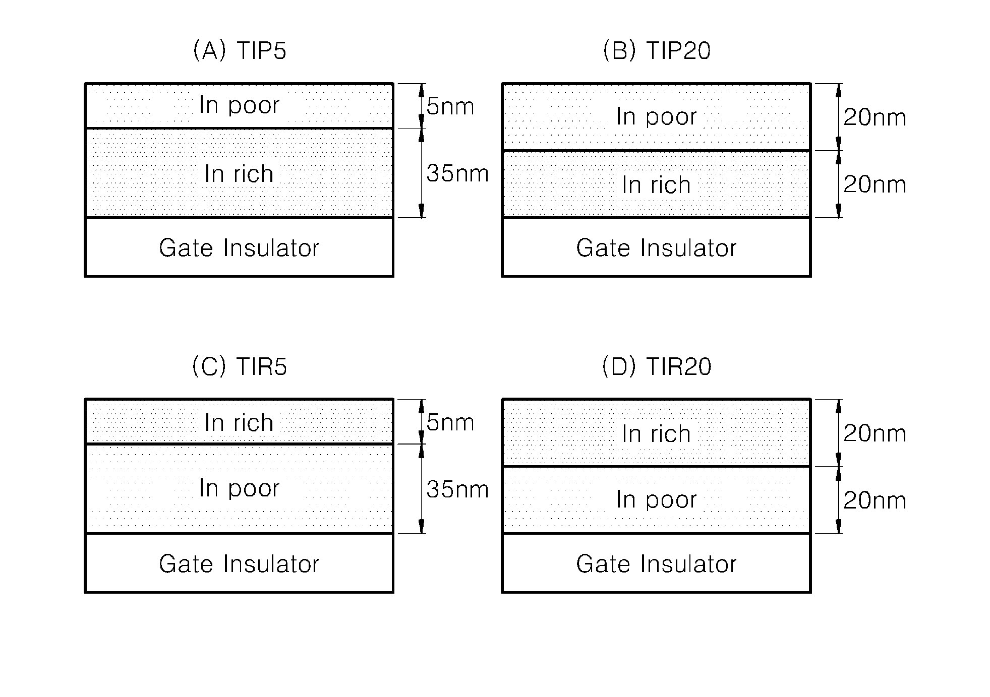
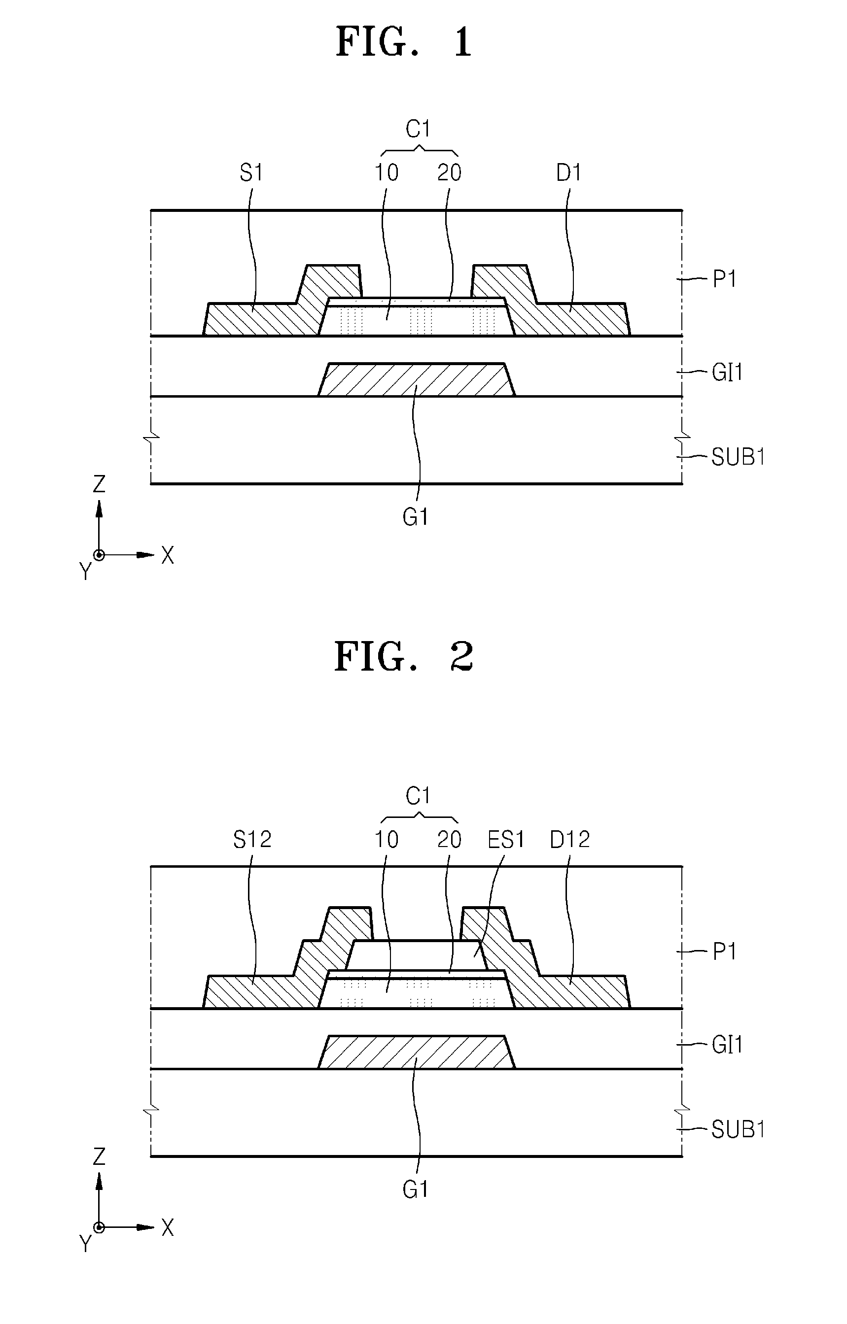
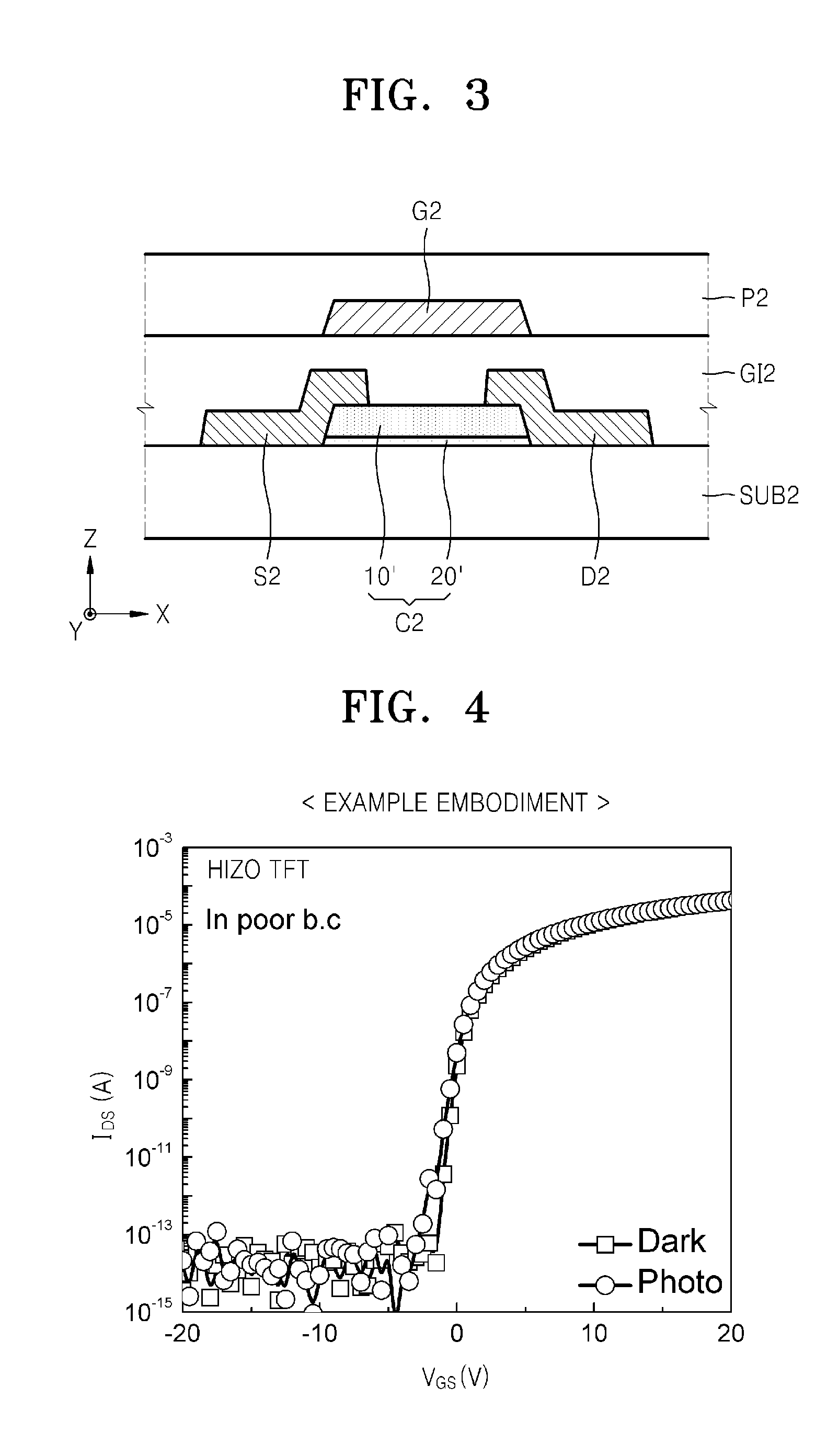
[0042]Various example embodiments will now be described more fully with reference to the accompanying drawings in which example embodiments are shown.

[0043]It will be understood that when an element is referred to as being “connected” or “coupled” to another element, it can be directly connected or coupled to the other element or intervening elements may be present. In contrast, when an element is referred to as being “directly connected” or “directly coupled” to another element, there are no intervening elements present. As used herein the term “and / or” includes any and all combinations of one or more of the associated listed items.

[0044]It will be understood that, although the terms “first”, “second”, etc. may be used herein to describe various elements, components, regions, layers and / or sections, these elements, components, regions, layers and / or sections should not be limited by these terms. These terms are only used to distinguish one element, component, region, layer or secti...


PUM


Abstract

An oxide transistor includes: a channel layer formed of an oxide semiconductor; a source electrode contacting a first end portion of the channel layer; a drain electrode contacting a second end portion of the channel layer; a gate corresponding to the channel layer; and a gate insulating layer disposed between the channel layer and the gate. The oxide semiconductor includes hafnium-indium-zinc-oxide (HfInZnO). An electrical conductivity of a back channel region of the channel layer is lower than an electrical conductivity of a front channel region of the channel layer.

Description

CROSS-REFERENCE TO RELATED APPLICATION(S)[0001]This application claims priority under 35 U.S.C. §119 to Korean Patent Application No. 10-2010-0115765, filed on Nov. 19, 2010, and Korean Patent Application No. 10-2010-0138043, filed on Dec. 29, 2010, in the Korean Intellectual Property Office, the disclosures of which are incorporated herein in their entirety by reference.BACKGROUND[0002]1. Field[0003]Example embodiments relate to transistors, methods of manufacturing the same, and electronic devices including transistors.[0004]2. Description of the Related Art[0005]Transistors are used as switching devices and driving devices in electronic devices. Because thin film transistors (TFTs) may be formed on glass substrates or plastic substrates, they are used in flat panel display apparatuses, such as liquid crystal display (LCD) devices, organic light emitting display (OLED) devices, and the like.[0006]To improve operating characteristics of TFTs, channel layers may be formed as oxide l...

Claims


Application Information

Patent Timeline
Patent Type & Authority Patents(United States)
IPC IPC(8): H01L29/786H01L29/10
CPCH01L29/7869
Inventor MAENG, WAN-JOORYU, MYUNG-KWANKIM, TAE-SANGPARK, JOON-SEOK
Owner SAMSUNG ELECTRONICS CO LTD
Why Eureka
Try Eureka