Photoelectric conversion element having a plurality of layered semiconductors and method for manufacturing same

a technology of photoelectric conversion element and semiconductor, applied in the direction of electrical apparatus, semiconductor devices, radio frequency control devices, etc., can solve the problems of increasing dark current and crack generation, and achieve the effects of increasing film thickness, increasing optical sensitivity, and reducing the number of cracks

Inactive Publication Date: 2015-02-10
SONY SEMICON SOLUTIONS CORP
View PDF2 Cites 2 Cited by
  • Summary
  • Abstract
  • Description
  • Claims
  • Application Information

AI Technical Summary

Benefits of technology

[0055]In the photoelectric conversion element 10, when a predetermined potential is applied from the power supply line (not shown) via the upper electrode 18, e.g. light incident from the side of the upper electrode 18 is converted to a signal charge with the amount of charge dependent on the amount of received light (photoelectric conversion). The signal charge generated by this photoelectric conversion is extracted as a photocurrent from the side of the p-type semiconductor layer 14.
[0056]In this photoelectric conversion element 10, the i-type semiconductor layer 16 is so provided as to be extended from the inside of the contact hole 150A to the top surface of the first interlayer insulating film 15A as described above. Thus, the i-type semiconductor layer 16 has the step structure 16S1 dependent on the difference in height of the wall surface 15S1 of the contact hole 150A. If the i-type semiconductor layer 16 has such a step structure 16S1, stress is applied to the i-type semiconductor layer 16 and a crack (seam) is easily generated at e.g. the edge part of the step structure 16S1. As described above, to enhance the optical sensitivity, it is preferable to increase the film thickness of the i-type semiconductor layer 16. However, as the film thickness is increased, the difference in height of the wall surface 15S1 becomes larger (difference in height of the step structure 16S1 becomes larger) and thus a crack is generated more easily.
[0057]The influence of the above-described crack in a photoelectric conversion element according to a comparative example (photoelectric conversion element 100) will be described below. FIG. 9 is a schematic plan view showing the forming area of a p-type semiconductor layer 104, a contact hole 109A, and an i-type semiconductor layer 106 (n-type semiconductor layer 107) in the photoelectric conversion element 100. FIG. 10A is a sectional view along line A-A′ in FIG. 9. FIG. 10B is an arrow sectional view along line B-B′. The photoelectric conversion element 100 has the p-type semiconductor layer 104 in a selective area over a substrate 101 with the intermediary of an insulating film 103, and a first interlayer insulating film 105A having the contact hole 109A opposed to the p-type semiconductor layer 104 is provided on the p-type semiconductor layer 104. The i-type semiconductor layer 106 and the n-type semiconductor layer 107 are provided in the area corresponding to the contact hole 109A, and the i-type semiconductor layer 106 has a step 106S in its top surface.
[0058]In the above-described photoelectric conversion element 100 of the comparative example, a crack X like that shown in FIG. 11A is generated due to stress attributed to the step 106S. The generated crack X reaches the p-type semiconductor layer 104. Thus, the crack X acts as a leakage path and the dark current is generated.
[0059]In contrast, in the present embodiment, the i-type semiconductor layer 16 has the corner part 16e as shown in FIG. 11B. Thus, the crack X is so generated that its start point (or end point) is the corner part 16e. Therefore, because the corner part 16e is not in contact with the p-type semiconductor layer 14, even when the crack X is generated attributed to the step structure 16S1, the crack X is led to the corner part 16e separate from the p-type semiconductor layer 14, so that acting of the crack X as a leakage path is suppressed. FIG. 12 is a picture obtained by photographing the actually generated crack X.
[0060]As described above, in the present embodiment, the i-type semiconductor layer 16 has the corner part 16e that is not in contact with the p-type semiconductor layer 14 in the PIN photodiode structure having the i-type semiconductor layer 16 between the p-type semiconductor layer 14 and the n-type semiconductor layer 17. Due to this feature, for example in the case in which the i-type semiconductor layer 16 has the step structure 16S1 dependent on the shape of the contact hole 150A, acting of a crack as a leakage path can be suppressed even when the crack is generated due to this step structure 16S1. This can suppress increase in the dark current attributed to the crack.

Problems solved by technology

Thus, stress is applied to the i-type semiconductor layer due to the shape of the hole (step of sidewall part) and a crack is generated.
Such a crack has a problem of acting as a leakage path and increasing the dark current.

Method used


Image

  • Photoelectric conversion element having a plurality of layered semiconductors and method for manufacturing same
  • Photoelectric conversion element having a plurality of layered semiconductors and method for manufacturing same
  • Photoelectric conversion element having a plurality of layered semiconductors and method for manufacturing same

Examples


application example (

4. Application Example (example of photoelectric conversion device and radiation imaging device using photoelectric conversion element)

embodiment

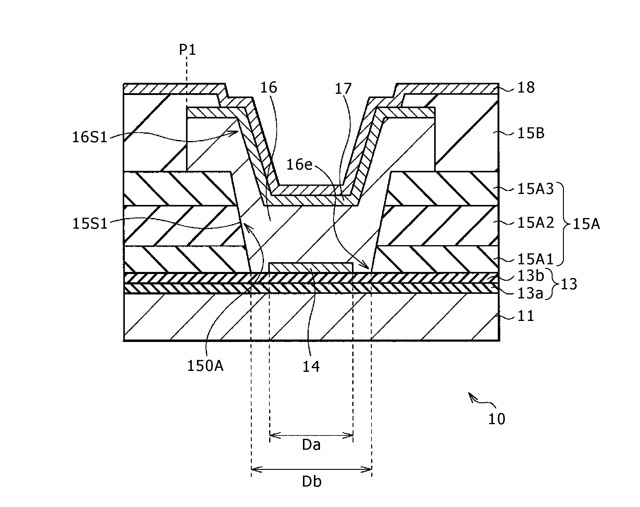
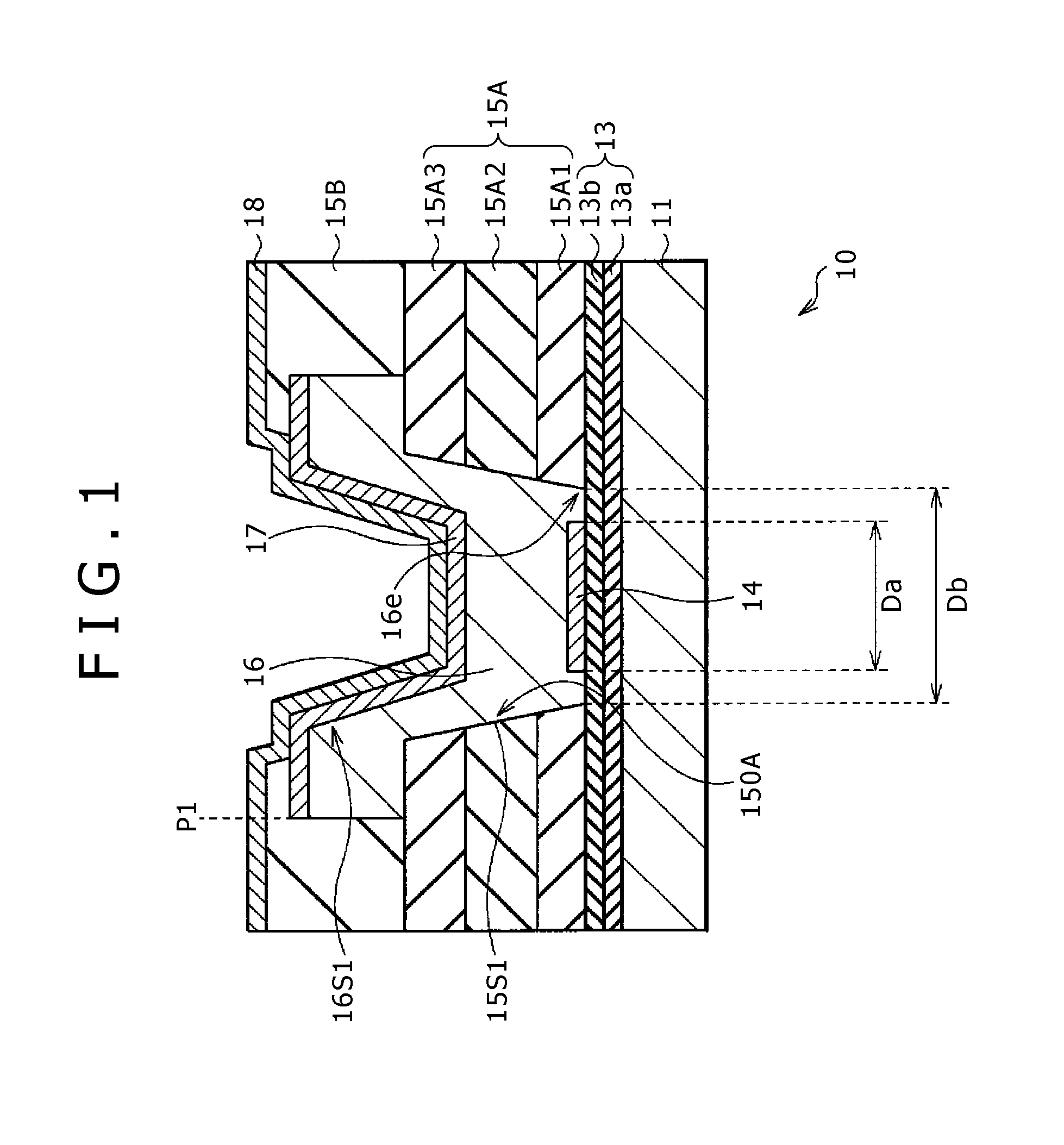
[0032]FIG. 1 shows the schematic configuration of a photoelectric conversion element 10 according to one embodiment of the present disclosure. The photoelectric conversion element 10 is a PIN (Positive Intrinsic Negative) photodiode obtained by interposing a non-doped i-type semiconductor layer (intrinsic semiconductor layer) between a p-type semiconductor layer and an n-type semiconductor layer.

[Whole Configuration of Photoelectric Conversion Element 10]

[0033]The photoelectric conversion element 10 has a p-type semiconductor layer 14 (first semiconductor layer) in a selective area over a substrate 11 composed of e.g. glass with the intermediary of an insulating film 13. Over the substrate 11 (specifically, on the insulating film 13), a first interlayer insulating film 15A having a contact hole 150A (through-hole) opposed to the p-type semiconductor layer 14 is provided. An i-type semiconductor layer 16 (third semiconductor layer) is provided on the p-type semiconductor layer 14 in ...

modification examples 1 and 2

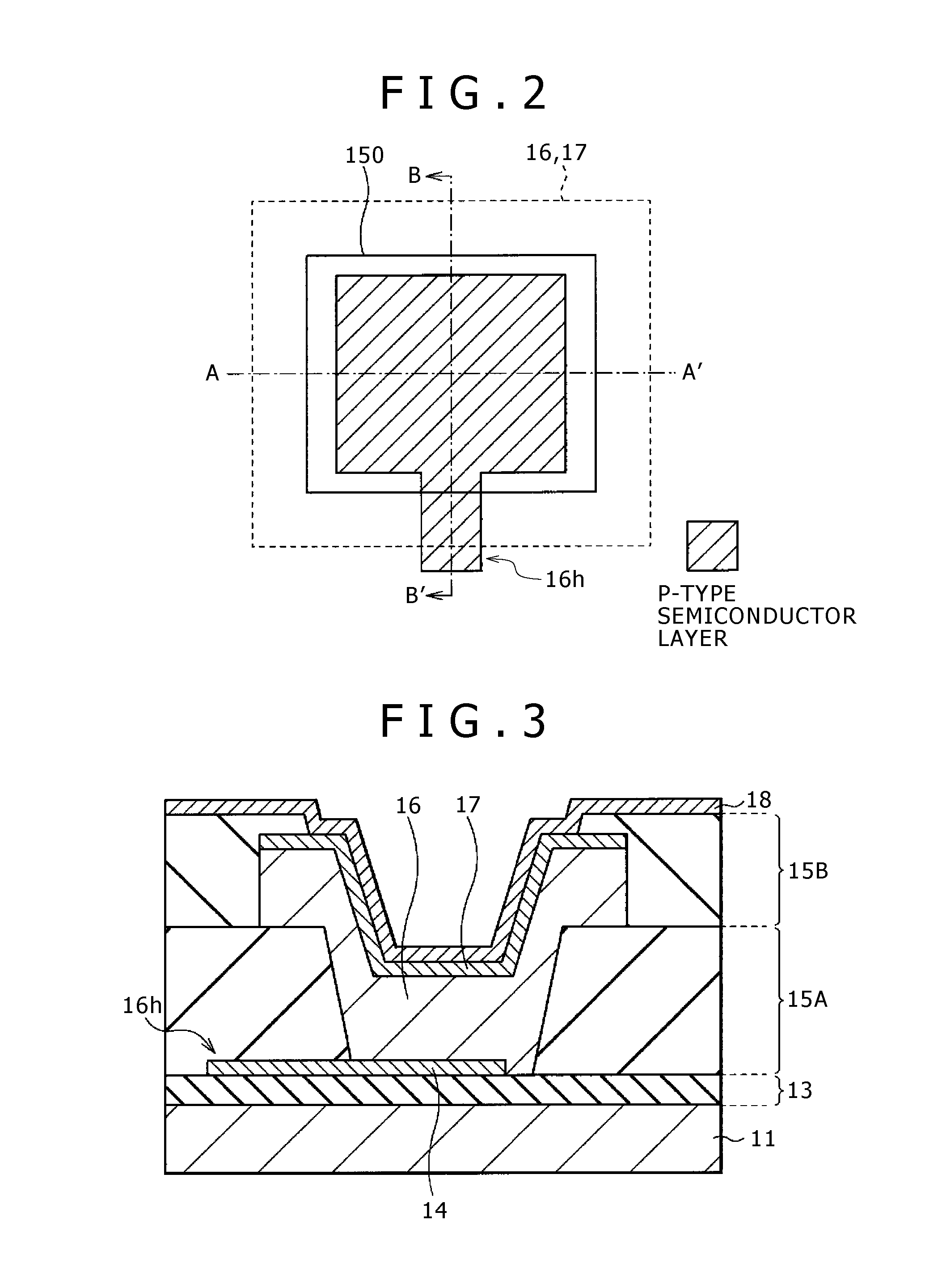
[0062]FIG. 13 shows the sectional configuration of a photoelectric conversion element according to modification example 1. FIG. 14 shows the sectional configuration of a photoelectric conversion element according to modification example 2. These photoelectric conversion elements of modification examples 1 and 2 have the p-type semiconductor layer 14 over the substrate 11 with the intermediary of the insulating film 13 and the i-type semiconductor layer 16 is provided in a contact hole 150C of a first interlayer insulating film 15C, similarly to the photoelectric conversion element 10 of the above-described embodiment. On the i-type semiconductor layer 16, the n-type semiconductor layer 17 is provided in accordance with the surface shape of the i-type semiconductor layer 16. In such a configuration, the i-type semiconductor layer 16 has a corner part that is not in contact with the p-type semiconductor layer 14. For simplification, diagrammatic representation of the second interlayer...


PUM


Abstract

A photoelectric conversion element includes a first semiconductor layer that exhibits a first conductivity type and is provided in a selective area over a substrate, a second semiconductor layer that exhibits a second conductivity type and is disposed opposed to the first semiconductor layer, and a third semiconductor layer that is provided between the first and second semiconductor layers and exhibits a substantially intrinsic conductivity type. The third semiconductor layer has at least one corner part that is not in contact with the first semiconductor layer.

Description

BACKGROUND[0001]The present disclosure relates to a photoelectric conversion element such as a PIN photodiode used for e.g. radiation imaging device and optical touch sensor, and a method for manufacturing the same.[0002]The PIN photodiode is used as a photoelectric conversion element in radiation imaging device, optical touch panel, etc. This PIN (Positive Intrinsic Negative) photodiode has a structure in which a so-called i-type semiconductor layer is interposed between a p-type semiconductor layer and an n-type semiconductor layer, and a signal charge with the amount of charge dependent on the amount of incident light can be extracted.[0003]Such a photodiode is desired to have further enhanced optical sensitivity and various proposals have been made for this desire (refer to e.g. Japanese Patent Laid-open No. 2000-156522). This patent document discloses a photoelectric conversion device in which a semiconductor layer in the photoelectric converter is extended to the transistor pa...

Claims


Application Information

Patent Timeline
Patent Type & Authority Patents(United States)
IPC IPC(8): H01L31/102H01L27/146H01L31/0352H01L31/105
CPCH01L31/0352H01L27/14663H01L31/105H01L27/14607H01L27/14692H01L31/18
Inventor YAMADA, YASUHIROTANAKA, TSUTOMUTAKATOKU, MAKOTOITO, RYOICHI
Owner SONY SEMICON SOLUTIONS CORP
Why Eureka
Try Eureka