Multi-level cell operation using zinc oxide switching material in non-volatile memory device

a zinc oxide switching material and multi-level cell technology, applied in static storage, information storage, digital storage, etc., can solve the problems of increasing power dissipation, reducing device performance, and non-scaling of sub-threshold slopes

Active Publication Date: 2015-03-03
CROSSBAR INC
View PDF39 Cites 13 Cited by
  • Summary
  • Abstract
  • Description
  • Claims
  • Application Information

AI Technical Summary

Benefits of technology

[0008]In a specific embodiment, a method of programming a non-volatile memory device is provided. The method includes providing a state-change device. In a specific embodiment, the state-change device includes a first electrode, a second electrode, and a state-change element configured in an intersection between the first electrode and the second electrode. In a specific embodiment, the first electrode comprises an aluminum doped zinc oxide material (commonly known as AZO), the state-change element comprises a zinc oxide material, and the second electrode comprises a silicon material having a p+ impurity characteristic. The method includes applying a first bias voltage to the first electrode of the as-fabricated state-change device to cause the state-change material to change from an as-fabricated state to a first state. The first bias voltage is characterized at least by a first amplitude. The as-fabricated state-change device is at least characterized by an as-fabricated resistance. The method includes applying a reverse bias voltage having an opposite polarity to the first bias voltage and having an amplitude substantially the same as the first amplitude to cause the state-change material to change from the first state to an off-state, the off-state being substantially the same as the as-fabricated state and having a resistance substantially the same as the as-fabricated state. The method includes applying a second bias voltage to the state-change device at the off-state. The second bias voltage is has a same polarity...

Problems solved by technology

However, as field effect transistors (FET) approach sizes less than 100 nm, problems such as the short channel effect degrade device performance.
Moreover, such sub 100 nm device sizes can lead to sub-threshold slope non-scaling and increase in power dissipation.
These devices often require new materials and device structures to couple with silicon-based devices to form a memory cell,...

Method used


Image

  • Multi-level cell operation using zinc oxide switching material in non-volatile memory device
  • Multi-level cell operation using zinc oxide switching material in non-volatile memory device
  • Multi-level cell operation using zinc oxide switching material in non-volatile memory device

Examples


Embodiment Construction

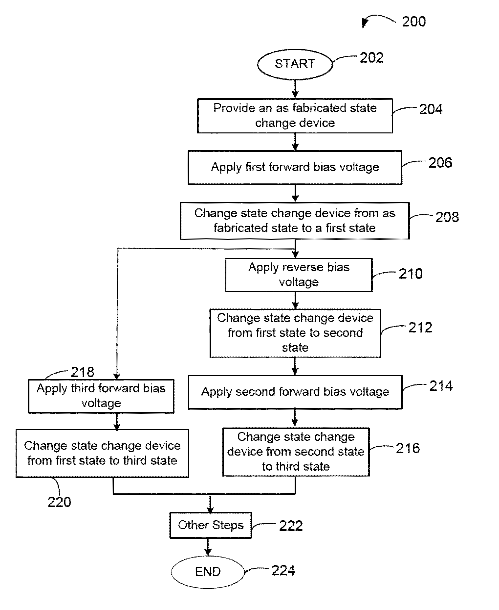
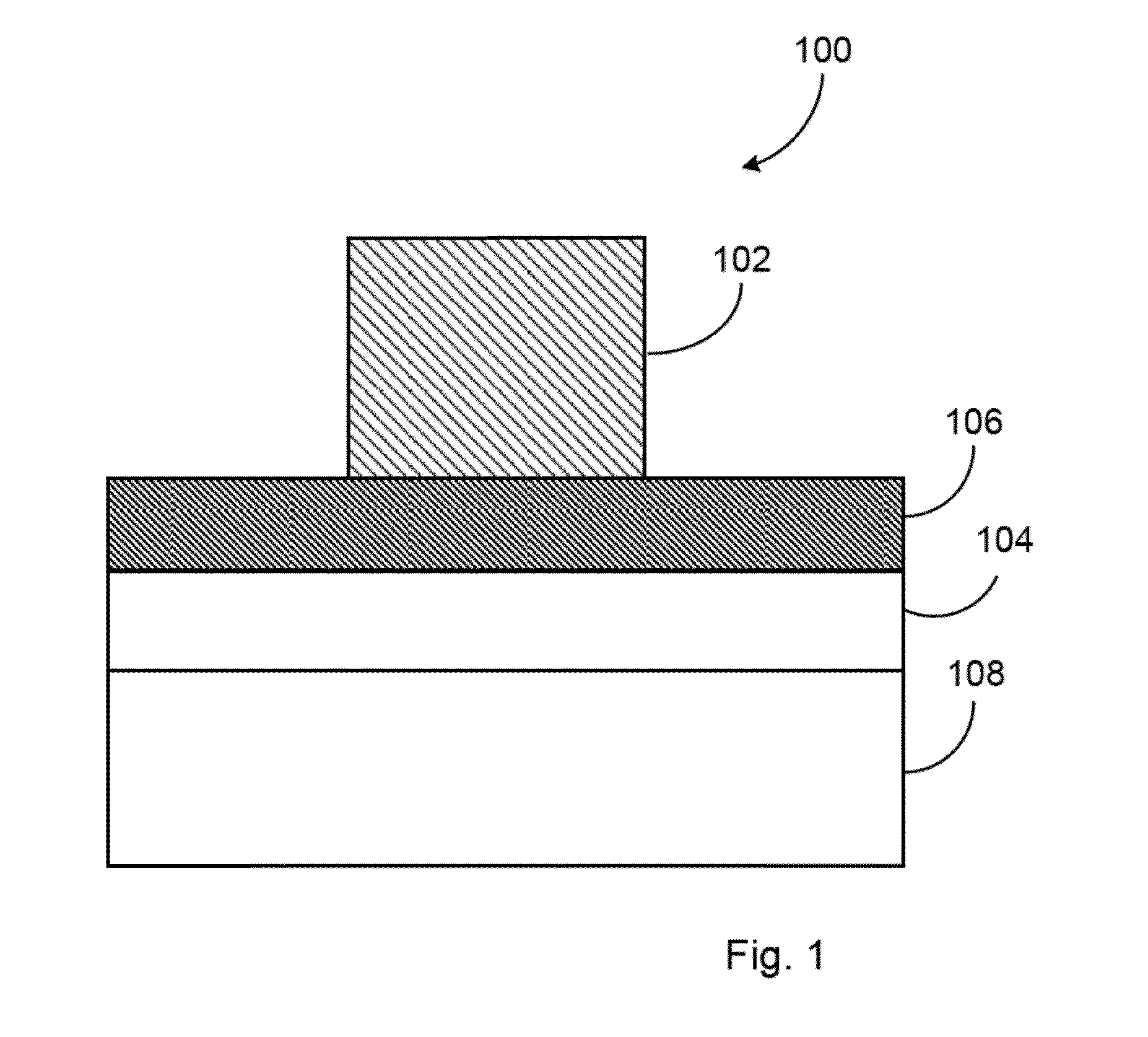
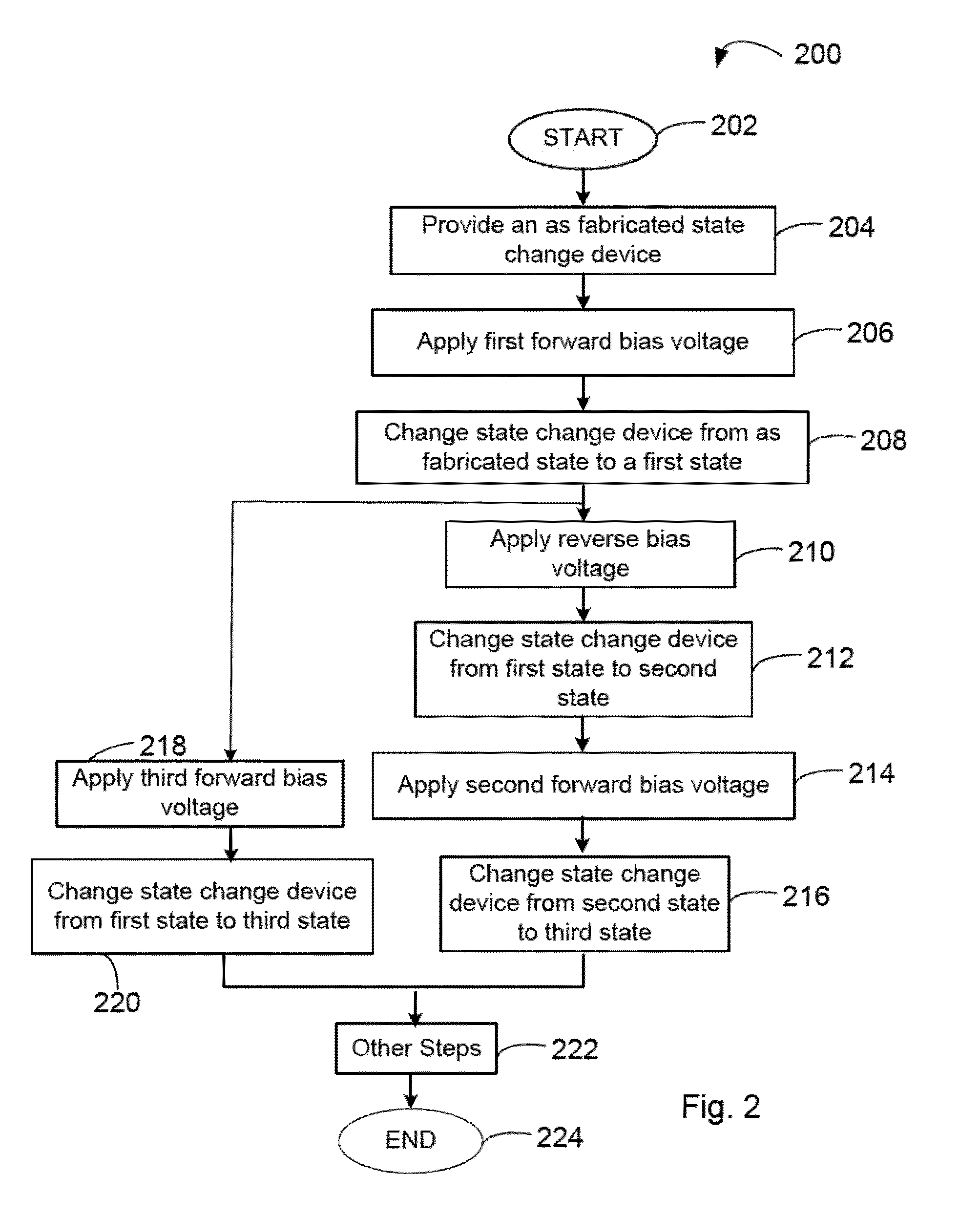
[0019]The present invention is generally related to state-change devices, for example, resistive switching devices. More particularly, embodiments according to the present invention provide a programming method for a multi-level cell. Embodiments of the present invention have been applied to non-volatile memory devices using aluminum doped zinc oxide (AZO) as a conductor material and a zinc oxide material as a switching material, but it should be recognized that the present invention can have a much broader range of applicability.

[0020]Embodiments of resistive random access memory devices can be programmed by applying a voltage across the electrodes to cause a resistance change in the resistive switching material or the state-change material. The resistance change or switching can be dependent on an amplitude and polarity of the voltage applied. Depending on the device and the resistive switching material, embodiments of multilevel devices can be achieved by applying voltages of dif...


PUM


Abstract

A method for programming a non-volatile memory device includes providing an as-fabricated state-change device having an aluminum doped zinc oxide material first electrode, a p++ polysilicon material second electrode, and a zinc oxide (ZnO) material state-change material there between. A first amplitude bias voltage is applied to the first electrode of the as-fabricated state-change device causing the ZnO material to change form an as-fabricated state to a first state. A second amplitude bias voltage having an opposite polarity having an amplitude similar to the first amplitude is applied to cause the ZnO to change from the first state to a second state substantially similar as the as-fabricated state. A third amplitude bias voltage having a same polarity to the first bias voltage and having an amplitude dissimilar to the first bias voltage is applied to cause the ZnO to change from the second state to a third state.

Description

CROSS REFERENCE TO RELATED APPLICATIONS[0001]Not Applicable.STATEMENT RELATED TO GOVERNMENT OR FEDERALLY FUNDED RESEARCH[0002]Not ApplicableBACKGROUND[0003]The present invention is generally related to state-change devices, for example, resistive switching devices. More particularly, embodiments according to the present invention provide a method to program a resistive switching device for a multi-level cell. The present invention can be applied to non-volatile memory devices but it should be recognized that the present invention can have a much broader range of applicability.[0004]The success of semiconductor devices has been mainly driven by an intensive transistor down-scaling process. However, as field effect transistors (FET) approach sizes less than 100 nm, problems such as the short channel effect degrade device performance. Moreover, such sub 100 nm device sizes can lead to sub-threshold slope non-scaling and increase in power dissipation. It is generally believed that trans...

Claims


Application Information

Patent Timeline
IPC IPC(8): G11C11/00
CPCG11C11/1675G11C11/2275G11C11/56G11C11/5628G11C11/5685G11C13/0002G11C13/0007G11C13/0069G11C2013/0073G11C2013/0083G11C2013/0092G11C2211/562G11C2211/5648G11C2213/15
Inventor JO, SUNG HYUNKUMAR, TANMAY
Owner CROSSBAR INC
Why Eureka
Try Eureka