
Method for annealing aluminum-doped zinc oxide transparent conductive thin film

A transparent conductive film, zinc oxide technology, applied in ion implantation plating, metal material coating process, coating, etc., can solve the problems of reducing the surface roughness of the film, increasing the surface roughness of the film, and deteriorating the conductive properties of the film , to achieve the effect of reducing film resistivity and improving mobility

Inactive Publication Date: 2011-03-16
FUJIAN INST OF RES ON THE STRUCTURE OF MATTER CHINESE ACAD OF SCI
View PDF1 Cites 13 Cited by
  • Summary
  • Abstract
  • Description
  • Claims
  • Application Information

AI Technical Summary

Problems solved by technology

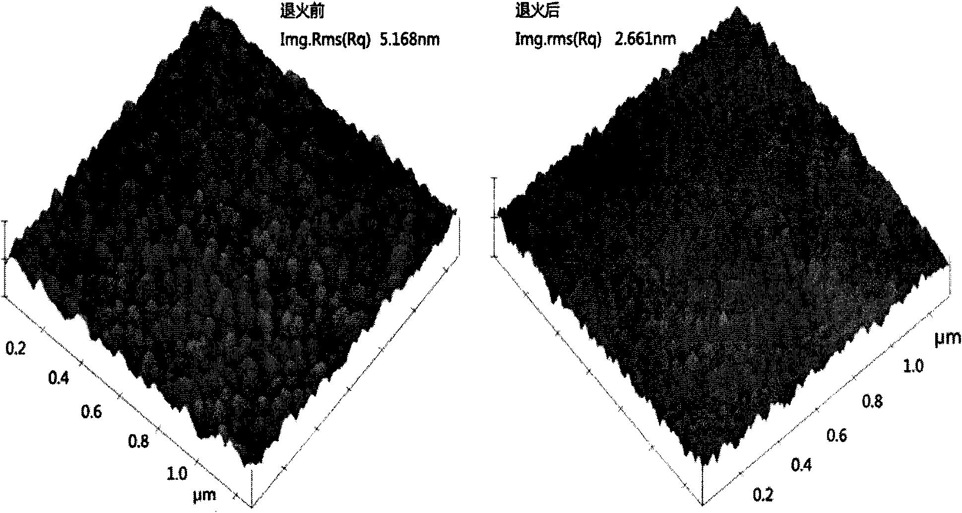
[0003] Existing studies have shown that annealing in an oxygen-containing atmosphere can improve the crystallization of transparent conductive films, reduce the surface roughness of the film and increase the transmittance of the film, but greatly deteriorate the conductive properties of the film; vacuum annealing can improve the conductive properties of the film, and Increase the surface roughness of the film; under an inert atmosphere such as argon, the crystallization of the AZO transparent conductive film can be improved, the surface roughness of the film can be reduced, and the introduction of hydrogen annealing can significantly improve the conductivity of the film
[0004] At present, most AZO-related patent documents focus on the production of AZO targets, and there is no patent report on annealing treatment

Method used


Image

  • Method for annealing aluminum-doped zinc oxide transparent conductive thin film
  • Method for annealing aluminum-doped zinc oxide transparent conductive thin film
  • Method for annealing aluminum-doped zinc oxide transparent conductive thin film

Examples


Embodiment 1

[0013] Embodiment 1: Co-sputtering low temperature, high speed deposition annealing AZO transparent conductive film

[0014] The quartz substrate was ultrasonically cleaned with acetone and alcohol, and then placed in a magnetron sputtering coating machine for reverse sputtering cleaning. The purity of the zinc oxide ceramic target for sputtering is 99.9%, the purity of the aluminum oxide target is 99.9%, and the relative density is greater than 90%. Install the targets in two opposing target guns, and evacuate until the background vacuum of the vacuum chamber is higher than 2.0×10 -4 Pa. The substrate temperature is kept at 200°C, and 20 sccm of argon gas is introduced into the vacuum chamber (sccm means standard milliliter per minute), and the pressure of the vacuum chamber is adjusted to 0.15Pa. The power of the RF power supply corresponding to the zinc oxide target is adjusted to 100W, and the corresponding The power of the RF power supply was adjusted to 75W, the sample...

Embodiment 2

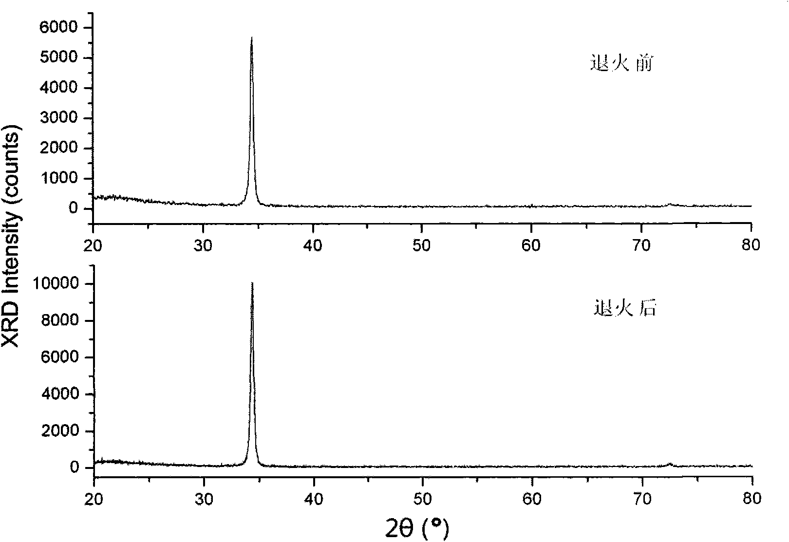
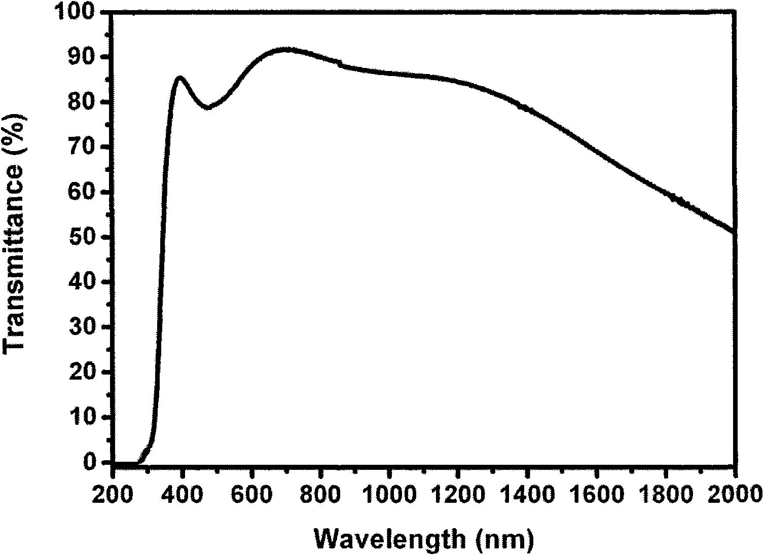
[0016] Put the sample deposited in Example 1 into the annealing furnace, turn on the mechanical pump to evacuate to 0.5 Pa, turn off the mechanical pump after 30 minutes, and feed 200 sccm of nitrogen gas to a slight positive pressure, raise the temperature to 300 ° C, turn off the nitrogen gas and feed in hydrogen gas, After annealing for 10 min, turn off the hydrogen gas and switch to nitrogen gas to lower the temperature. Tests show that the mass ratio of aluminum content to the sum of aluminum content and zinc content in the AZO transparent conductive film [W Al / (W Al +W Zn )]≈2%, its crystal structure is a hexagonal wurtzite phase structure along the (002) orientation, and its resistivity is 5.94×10 -4 Ω·cm, the sheet resistance is 29.71Ω / □, and the carrier concentration is 1.88×10 21 / cm 3 , with a mobility of 5.61cm 2 V -1 S -1 , The average transmittance is greater than 80% in the wavelength range of 400-1000nm, and the surface roughness is 2.7nm.

Embodiment 3

[0018] Put the sample deposited in Example 1 into the annealing furnace, turn on the mechanical pump to evacuate to 0.5Pa, pass in 300sccm argon to a slight positive pressure, raise the temperature to 200°C and keep it for 30min, then change the flow to 100sccmH 2 and 200sccmN 2 After annealing for 20 minutes, turn off the hydrogen gas, and switch to argon gas to cool down. The test shows that the crystal structure of the AZO transparent conductive film is a hexagonal wurtzite phase structure along the (002) orientation, and the resistivity is 4.30×10 -4 Ω cm, the sheet resistance is 21.52Ω / □, and the carrier concentration is 1.22×10 21 / cm 3 , with a mobility of 12.83cm 2 V -1 S -1 , The average transmittance is greater than 80% in the wavelength range of 400-1000nm, and the surface roughness is 2.1nm.


PUM

PropertyMeasurementUnit
Resistivityaaaaaaaaaa
Sheet resistanceaaaaaaaaaa
Surface roughnessaaaaaaaaaa

Abstract

The invention relates to a method for annealing an aluminum-doped zinc oxide (AZO) transparent conductive thin film. In the method, the AZO transparent conductive film is annealed by introducing a certain amount of inert gas (such as nitrogen gas, argon gas and the like), reducing gas (hydrogen gas, methane and the like) or mixed gas of the inert gas and the reducing gas into an annealing furnace under vacuum. By annealing, the mobility and the carrier concentration are obviously improved, so that the resistivity of the thin film is reduced; and the crystallization of the annealed thin film is improved, and a good C-axis preferred orientation structure is kept. By the method, the AZO transparent conductive thin film rapidly grows in a magnetron sputtering coating machine at a low temperature and then is annealed in the annealing furnace in batches, so that the performance of the AZO transparent conductive thin film is improved, and the production efficiency of the AZO transparent conductive thin film is greatly improved.

Description

technical field [0001] The invention relates to an annealing method for an aluminum-doped zinc oxide transparent conductive film, and belongs to the technical field of optoelectronic functional materials. technical background [0002] Transparent conductive oxide (TCO for short) has extremely important applications in the field of optoelectronic technology. Tin-doped indium oxide (ITO) transparent conductive films have been intensively studied and widely used in flat panel displays, solar cells, and LEDs. Aluminum-doped zinc oxide (AZO) has attracted widespread attention due to its better thermal stability and more stable properties in hydrogen plasma. It is more suitable for thin-film solar cell electrode materials than ITO. In addition, compared with ITO, the biggest advantage of AZO is that the raw materials are environmentally friendly and cheap. With the deepening of research, AZO is expected to replace ITO in some application fields. [0003] Existing studies have s...

Claims


Application Information

Patent Timeline
IPC IPC(8): C23C14/56C23C14/06C23C14/35
Inventor 曹永革邓种华黄常刚
Owner FUJIAN INST OF RES ON THE STRUCTURE OF MATTER CHINESE ACAD OF SCI
Learn More