Composite back reflection metal electrode for thin film solar cell, as well as preparation method and application of composite back reflective metal electrode
A technology of thin-film solar cells and metal electrodes, which is applied in the manufacture of circuits, electrical components, and final products. The effect of peeling off and improving adhesion
- Summary
- Abstract
- Description
- Claims
- Application Information
AI Technical Summary
Problems solved by technology
Method used
Image
Examples
Embodiment 1
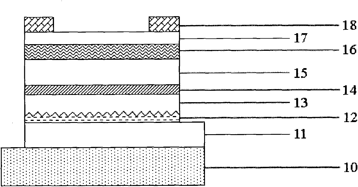
[0030] figure 1 A schematic diagram of the structure of a single-junction silicon-based thin-film solar cell comprising a composite back-reflecting metal electrode of the present invention is provided. According to the present invention, the main steps of preparing the main body of the solar cell are as follows:
[0031] The first step: put the prepared substrate containing the metal transition layer (nickel or cadmium or copper or titanium), the textured silver film, and the aluminum-doped zinc oxide barrier layer into the plasma-enhanced chemical vapor deposition system, the substrate Bake at 200°C for 1 hour;
[0032] The second step: sequentially deposit n, i, p three layers of silicon-based films in different chambers;
[0033] Step 3: Cool down to room temperature, take out the sample; place the sample prepared with silicon-based thin film in the coating system, and prepare aluminum-doped zinc oxide, tin dioxide or indium tin oxide transparent conductive film;
[0034]...
Embodiment 2
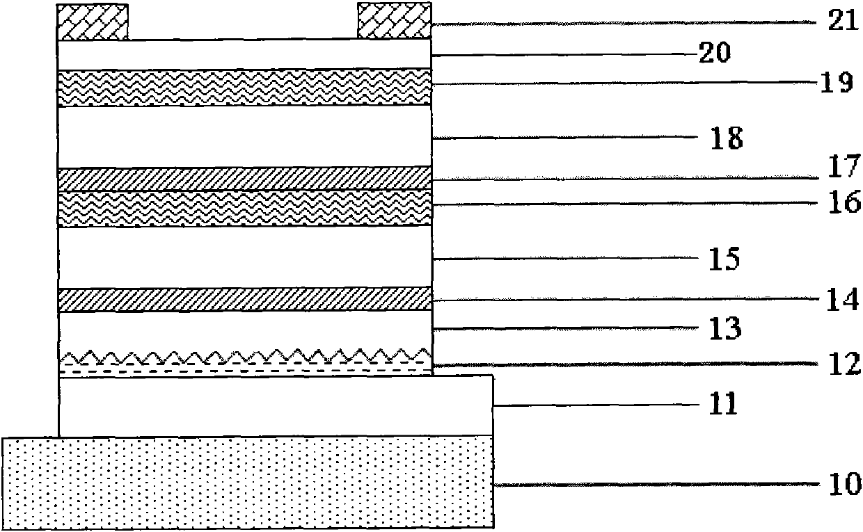
[0038] image 3A schematic structural view of a multi-junction silicon-based thin-film solar cell comprising a composite back-reflecting metal electrode of the present invention is provided. According to the present invention, the main steps of preparing the solar cell body are as follows:
[0039] The first step: put the prepared substrate containing the metal transition layer (nickel or cadmium or copper or titanium), the textured silver film, and the aluminum-doped zinc oxide barrier layer into the plasma-enhanced chemical vapor deposition system, the substrate Bake at 200°C for 1 hour;
[0040] The second step: sequentially deposit n, i, p three layers of silicon-based films 14-16 in different chambers;
[0041] Step 3: sequentially deposit n, i, p three layers of silicon-based films 17-19 in different chambers;
[0042] Step 4: Cool down to room temperature, take out the sample; place the sample prepared with silicon-based thin film in the coating system, and prepare al...
PUM
| Property | Measurement | Unit |
|---|---|---|
| thickness | aaaaa | aaaaa |
| thickness | aaaaa | aaaaa |
Abstract
Description
Claims
Application Information
 - R&D
- Intellectual Property
- Life Sciences
- Materials
- Tech Scout
- Unparalleled Data Quality
- Higher Quality Content
- 60% Fewer Hallucinations
Browse by: Latest US Patents, China's latest patents, Technical Efficacy Thesaurus, Application Domain, Technology Topic, Popular Technical Reports.
© 2025 PatSnap. All rights reserved.Legal|Privacy policy|Modern Slavery Act Transparency Statement|Sitemap|About US| Contact US: help@patsnap.com


