Single-poly non-volatile memory cell

a single-poly, non-volatile technology, applied in the direction of semiconductor devices, electrical equipment, transistors, etc., can solve the problems of inability to erase electrical data, slow programming, high voltage operation of conventional single-poly nvm, etc., to achieve shrinkable and scalable structure, high coupling ratio, and high coupling ratio

Inactive Publication Date: 2015-03-10
CHEN WANG YU HSIU
View PDF32 Cites 11 Cited by
  • Summary
  • Abstract
  • Description
  • Claims
  • Application Information

AI Technical Summary

Benefits of technology

[0011]It is one object of this invention to provide a single-poly, one-transistor one-capacitor (1T1C) NVM cell with high coupling ratio, which is compatible with current CMOS logic processes with minor change by adding one process layer, and which has a shrinkable and scalable structure for deep sub-micron dimensions, preferably 65 nm technology nodes and beyond.

Problems solved by technology

Although compatible with standard CMOS fabrication, conventional single-poly NVM suffers from high-voltage operation, slow programming, and incapability of electrical erase.
As a result, the drive current and / or coupling ratio are usually insufficient to effectively perform operations such as programming, erasing and reading.

Method used


Image

  • Single-poly non-volatile memory cell
  • Single-poly non-volatile memory cell
  • Single-poly non-volatile memory cell

Examples


Embodiment Construction

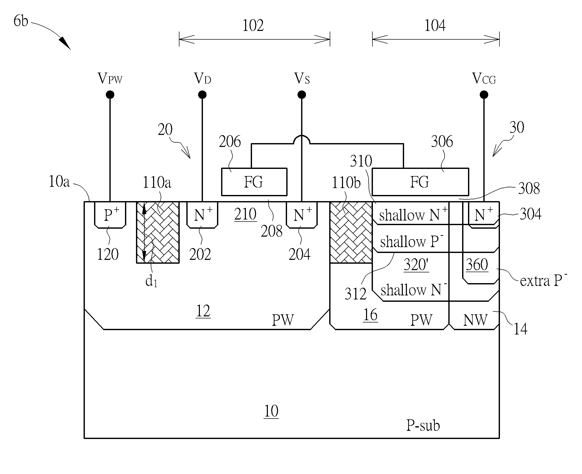
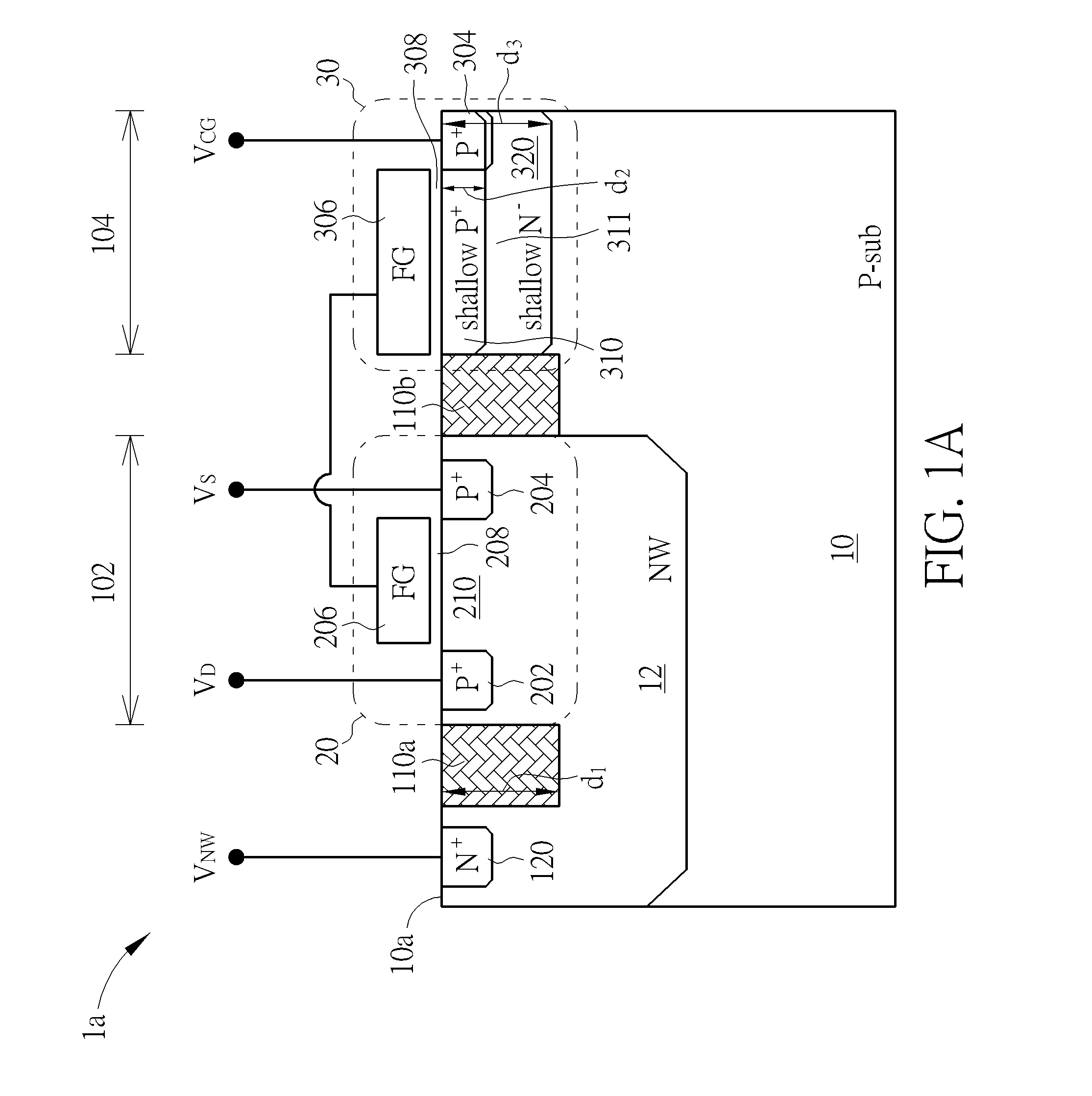
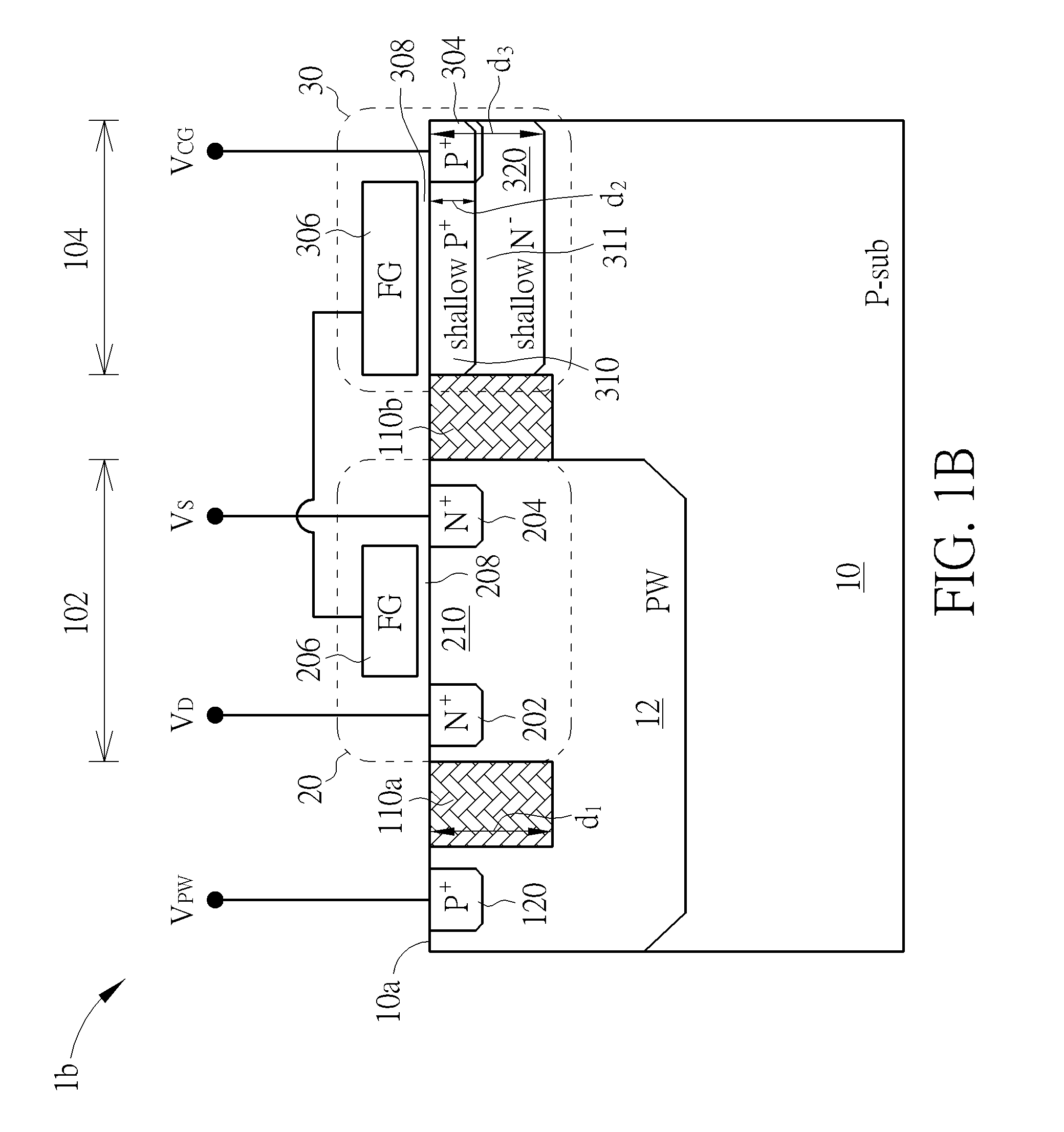
[0046]In the following detailed description of the invention, reference is made to the accompanying drawings, which form a part hereof, and in which is shown, by way of illustration, specific embodiments in which the invention may be practiced. These embodiments are described in sufficient detail to enable those skilled in the art to practice the invention. Other embodiments may be utilized and structural, logical, and electrical changes may be made without departing from the scope of the present invention.

[0047]The terms “wafer” and “substrate” used herein include any structure having an exposed surface onto which at least a layer is deposited according to the present invention, for example, to form the integrated circuit (IC) structure. The term “substrate” is understood to include semiconductor wafers. The term “substrate” is also used to refer to semiconductor structures during processing, and may include other layers that have been fabricated thereupon. Both wafer and substrate...


PUM


Abstract

A single-poly NVM cell includes a substrate having an isolation region separating a first OD region from a second OD region, a read transistor within the first OD region, and a coupling capacitor within the second OD region. A first ion well completely overlaps with the first oxide define region. The read transistor includes a drain region, a source region, a channel region, a single-poly floating gate overlying the channel region, and a gate dielectric layer between the floating gate and the channel region. The coupling capacitor includes a shallow ion well, a heavily-doped, ultra-shallow dopant region in the shallow ion well, a single-poly charge-storage floating gate overlying the heavily-doped, ultra-shallow dopant region, and a gate dielectric layer under the charge storage floating gate. The shallow ion well has a junction depth that is substantially equal to or shallower than a trench depth of the isolation region.

Description

CROSS REFERENCE TO RELATED APPLICATIONS[0001]This application claims priority from U.S. provisional application Ser. No. 61 / 875,700 filed Sep. 10, 2013, U.S. provisional application Ser. No. 61 / 876,775 filed Sep. 12, 2013, U.S. provisional application Ser. No. 61 / 882,024 filed Sep. 25, 2013, U.S. provisional application Ser. No. 61 / 887,470 filed Oct. 7, 2013, and U.S. provisional application Ser. No. 61 / 892,425 filed Oct. 17, 2013, which are incorporated herein by reference in their entirety.BACKGROUND OF THE INVENTION[0002]1. Field of the Invention[0003]The present invention relates generally to non-volatile memory (NVM) devices. More particularly, the present invention relates to a single polycrystalline silicon (single-poly) NVM cell.[0004]2. Description of the Prior Art[0005]Nonvolatile memory (NVM) devices are well known in the art. A NVM device does not lose its data when the system or device is turned off. As the demand for small size portable electrical devices such as cellu...

Claims


Application Information

Patent Timeline
Patent Type & Authority Patents(United States)
IPC IPC(8): H01L27/108H01L27/115H01L29/94
CPCH01L27/11558H01L29/94H10B41/60
Inventor CHEN, CHI-TSAI
Owner CHEN WANG YU HSIU
Why Eureka
Try Eureka