Electronic device and noise current measuring method

a technology of electronic devices and noise current, applied in the direction of noise figure or signal-to-noise ratio measurement, electrical apparatus casings/cabinets/drawers, instruments, etc., can solve the problems of malfunction due to static electricity, countermeasure costs, and increase in the environment of electronic devices, so as to enhance the reliability of electronic devices and suppress emi

Inactive Publication Date: 2015-03-17
HITACHI LTD
View PDF16 Cites 3 Cited by
  • Summary
  • Abstract
  • Description
  • Claims
  • Application Information

AI Technical Summary

Benefits of technology

[0032]According to the present invention, electrostatic resistance characteristics or like immunity tolerance of an electronic device such as an information processor, an information appliance, or a storage device can be improved to enhance reliability of the electronic device, without adding a countermeasure component to a printed PCB or PWB mounted on the electronic device. In addition, the present invention can suppress EMI from the electronic device.

Problems solved by technology

Thus, the environment of the electronic device regarding static electricity is becoming severe from year to year.
Countermeasure costs needed to pass the above-mentioned electrostatic test tend to increase as well.
Further, malfunctions due to static electricity occur even in the devices that have passed the test, which is now a major problem.
This is because, particularly in an electrostatic issue, the noise current caused by electrostatic discharge may flow from the enclosure via the screw / spacer to the PCB or PWB, and the noise current that has flown into the PCB or PWB may be released to the enclosure via the screw / spacer.
The noise current generated in a semiconductor such as LSI flows from the PCB or PWB via the screw / spacer portion into the enclosure, thereby causing EMI.

Method used


Image

  • Electronic device and noise current measuring method
  • Electronic device and noise current measuring method
  • Electronic device and noise current measuring method

Examples


embodiment 1

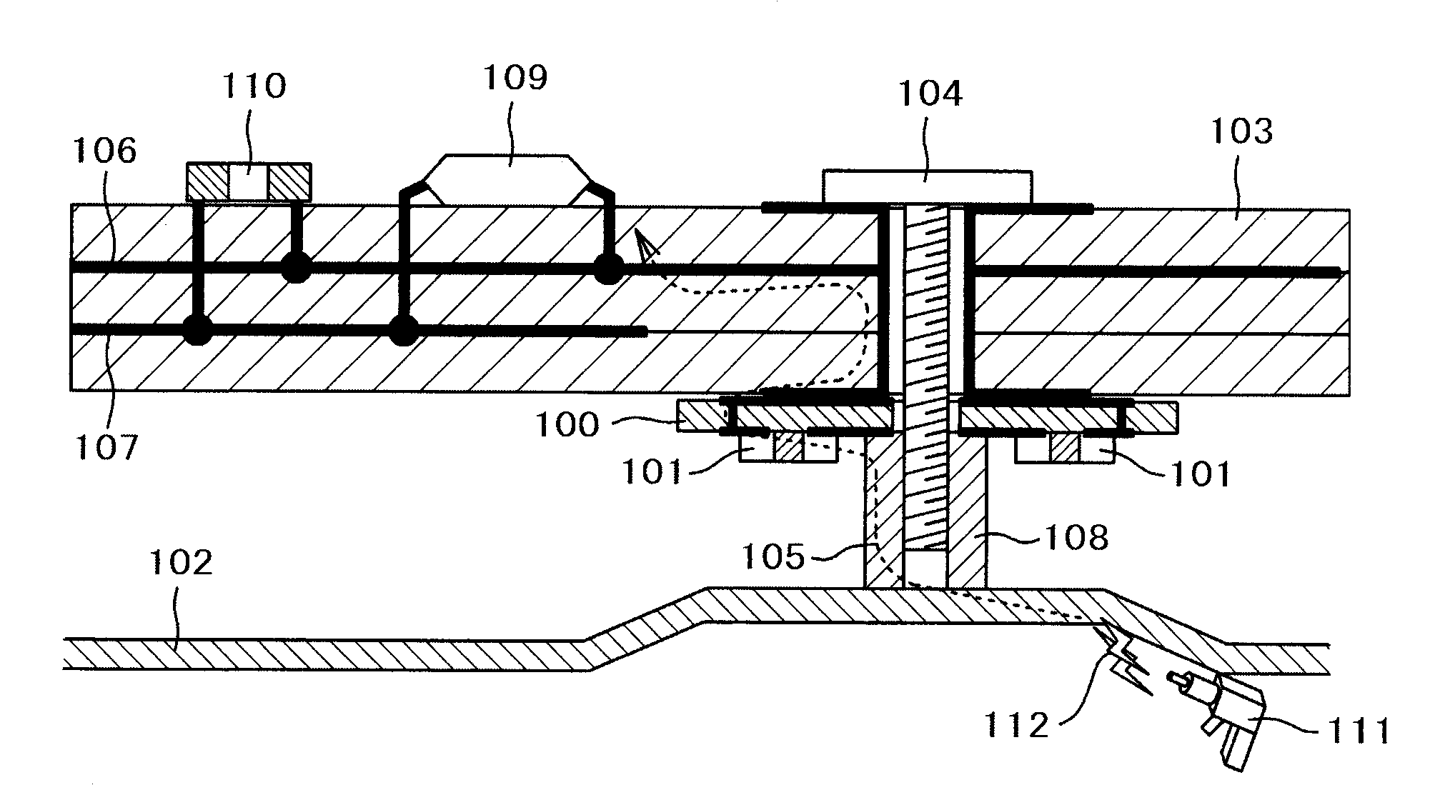
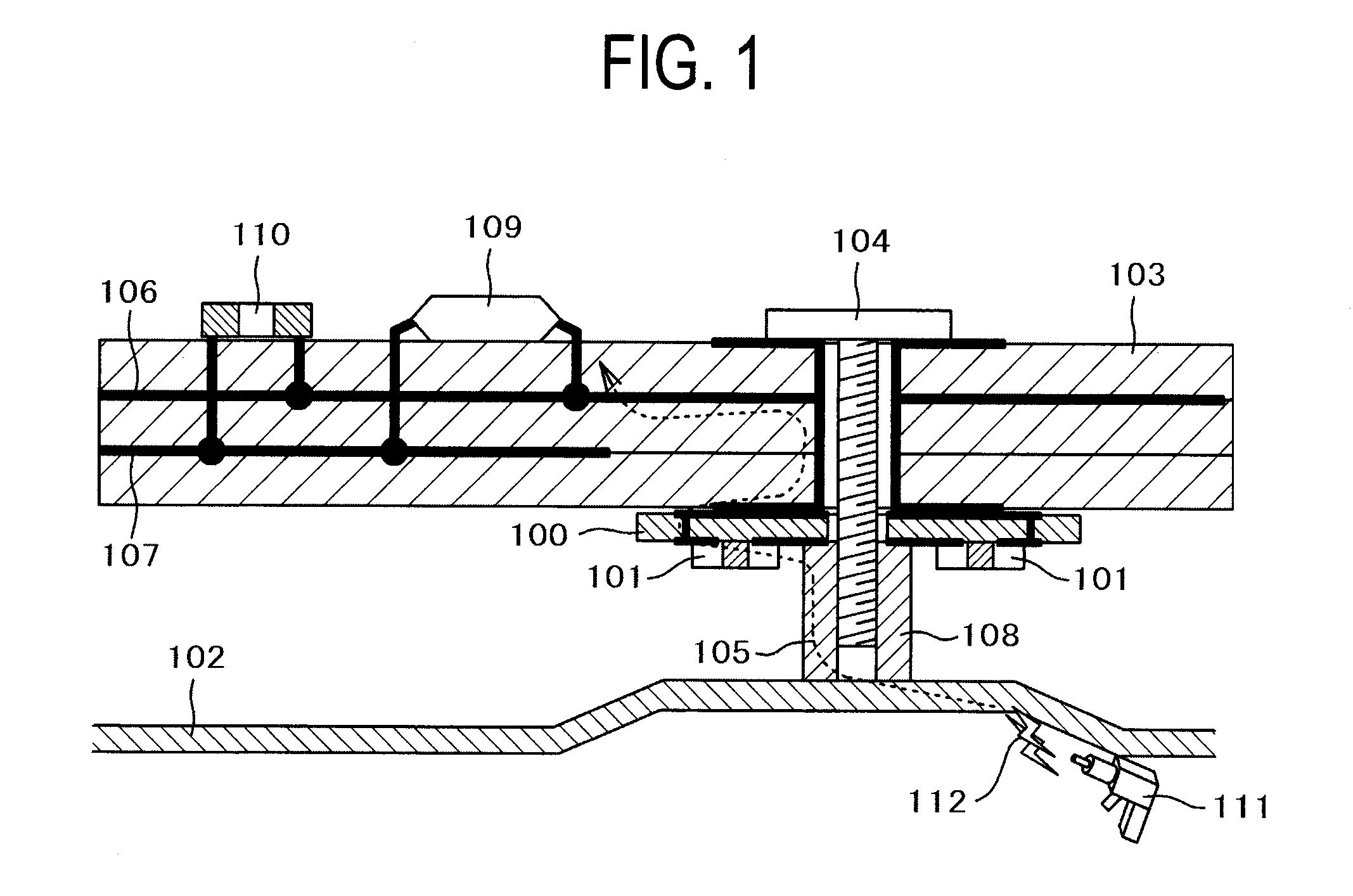
[0056]FIG. 1 is a cross-sectional view of a device on which an electrostatic noise suppression component is mounted, illustrating a typical embodiment of the present invention.

[0057]A problem in a conventional electrostatic test is described using FIG. 16 before the description of the embodiments of the present invention. FIG. 16 is a cross-sectional view of an electronic device in which a metal enclosure 102 and a PCB or PWB 103 are secured via a metal spacer 108 by means of a screw 104. The PCB or PWB 103 has a ground trace 106 and a power trace 107, and an LSI (Large Scale Integrated Circuit) 109 and a bypass capacitor 110 are mounted thereon.

[0058]As mentioned in “Background Art”, in the electrostatic test specified in IEC61000-4-2, electrostatic noise 112 is applied to a portion of an electronic device where people touch, a metal enclosure in FIG. 16 for example, by use of an ESD (Electrostatic Discharge) gun 111. The noise current 105 occurring at this time flows from the meta...

embodiment 2

[0075]An embodiment of a noise suppression component 100 according to the present invention is described in detail with reference to FIGS. 4A to 8B. FIGS. 4A to 7B shows noise suppression components configured to have substantially the same size and shape as those of the metal washer 901. FIGS. 8A and 8B show a noise suppression component having the same configuration as that of the screw 104. Each of them can be employed by replacing them with the conventionally used metal washer 901 and screw 104.

[0076]Details of FIGS. 4A to 5B are first described. FIGS. 4A and 5A are plan views of the noise suppression component 100 and FIGS. 4B and 5B are cross-sectional views of the noise suppression component 100. An upper portion and a lower portion of the noise suppression component 100 are respectively defined as a surface A and a surface B in the cross-sectional views of FIGS. 4B and 5B.

[0077]The noise suppression component 100 is composed of a threaded hole 400 adapted to receive a screw ...

embodiment 3

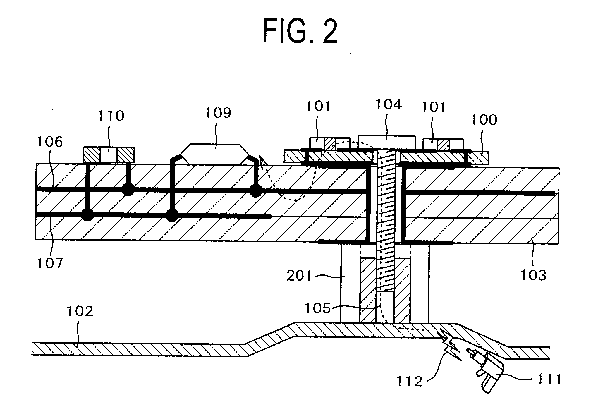
[0094]Embodiment 3 describes a probe for noise measurement and a measuring method of the measurement. The washer-type noise suppression components 100 shown in FIGS. 4A-7B can be utilized as noise measurement probes by modifying the configurations thereof. The use of the noise measurement probe makes it possible to measure the noise current 105 flowing into the PCB or PWB 103 from the metal enclosure 102 via the metal spacer 108 and the screw 104.

[0095]One example of the embodiment of the probe structure for measuring an electric current flowing into a joint portion between the metal enclosure 102 and the PCB or PWB 103 is described by use of FIGS. 10A and 10B. FIG. 10A is a plan view of a resistance detection screw current probe 1000 and FIG. 10B is a cross-sectional view of the resistance detection screw current probe 1000.

[0096]The resistance detection screw current probe 1000 shown in FIGS. 10A and 10B is provided by modifying and transforming the noise suppression component 100...


PUM


Abstract

A noise current passing through a substrate on which an electronic component is mounted is suppressed in a housing, to provide a malfunction of an electronic device. A substrate (103) on which an electronic component is mounted is secured to a housing (102) by a metal spacer (108) and a screw (104). A noise control member (100) mainly composed of an insulation substance is disposed between the metal spacer (108) and the substrate (103). A first conductive film is formed on the metal spacer-side of the noise control member (100), and a second conductive film is formed on the substrate-side of the noise control member (100). A resistance member (101) is disposed between the first conductive film and the second conductive film. A noise current introduced from the housing to the substrate can be suppressed by the resistance member.

Description

TECHNICAL FIELD[0001]The present invention relates to an electronic device that is configured to prevent an electronic component disposed on a PCB (Printed Circuit Board) or PWB (Printed Wiring Board) inside an enclosure from breakdown or malfunction due to noise such as static electricity. The invention also relates to a method of measuring a noise current caused by static electricity or the like applied to the electronic device.BACKGROUND ART[0002]Electronic devices such as consumer devices, manufacturing devices, and inspecting devices are specified to undergo an immunity tolerance test (IEC61000-4-2). The immunity test aims to confirm that the electronic device will not malfunction even if it is subjected to electrostatic discharge caused by people touching a portion of the electronic device or aerial discharge. Recently, immunity tolerance of semiconductors has deteriorated since operating margin has been reduced for lower source voltage, and non-metalization of enclosures has ...

Claims


Application Information

Patent Timeline
Patent Type & Authority Patents(United States)
IPC IPC(8): G01R29/26G01R31/08G01R31/00G01R31/28H05K1/02H05K1/14H05K3/32H05K9/00
CPCG01R31/001G01R29/26G01R31/281H05K1/0234H05K9/0039H05K9/0069H05K2201/10409H05K2201/2036H05K2201/10022H05K1/141H05K3/325H05K1/0215G01R31/00H05K9/00
Inventor NAKAMURA, SATOSHISUGA, TAKASHIUEMATSU, YUTAKA
Owner HITACHI LTD
Why Eureka
Try Eureka