Curved-surface display panel fabrication method, curved-surface display panel using same, and multi-image display device using same

a technology of curved surfaces and display panels, applied in the manufacture of electric discharge tubes/lamps, electric apparatus casings/cabinets/drawers, instruments, etc., can solve the problems of high manufacturing cost, difficult manufacturing process of conventional flexible liquid crystal display panels, and inability to use curved displays. , to achieve the effect of reducing thicknesses, simple process and simplified assembly process of multi-image display devices

Active Publication Date: 2015-03-17
TOVIS
View PDF29 Cites 153 Cited by
  • Summary
  • Abstract
  • Description
  • Claims
  • Application Information

AI Technical Summary

Benefits of technology

[0028]According to the present invention, outer surfaces of the first substrate and the second substrate of a conventional flat display panel are partially removed to reduce the thicknesses thereof and then the display panel is bent, and guide members are attached to the first substrate and the second substrate and the light transmitting reinforcing layer is formed to maintain the curved shape, so the curved-surface display panel can be fabricated through simple process.
[0029]Further, by using the curved-surface display panel as a rear display of a multi-image display device, the occurrence of the interference pattern (Moire phenomenon) due to the interference of the different pixel patterns can be prevented, and since an additional diffuse layer is not needed, the assembling process of the multi-image display device can be simplified.

Problems solved by technology

Such a liquid crystal display panel is generally manufactured in a flat shape, so the conventional liquid crystal display panel cannot be used as a curved display.
However, there is a problem that the manufacturing process of the conventional flexible liquid crystal display panel is difficult and the manufacturing cost thereof is high.
In this case, there is a problem that a noise (interference pattern) such as wood grain and water wave due to the interference between the overlapped LCD panels occurs.
That is, if a plurality of LCD panels having cross stripes by pixels are closely disposed, a noise occurs by the Moire phenomenon.

Method used


Image

  • Curved-surface display panel fabrication method, curved-surface display panel using same, and multi-image display device using same
  • Curved-surface display panel fabrication method, curved-surface display panel using same, and multi-image display device using same
  • Curved-surface display panel fabrication method, curved-surface display panel using same, and multi-image display device using same

Examples


Embodiment Construction

Technical Problem

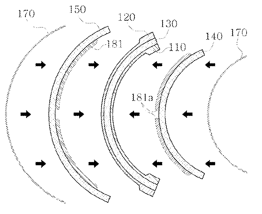
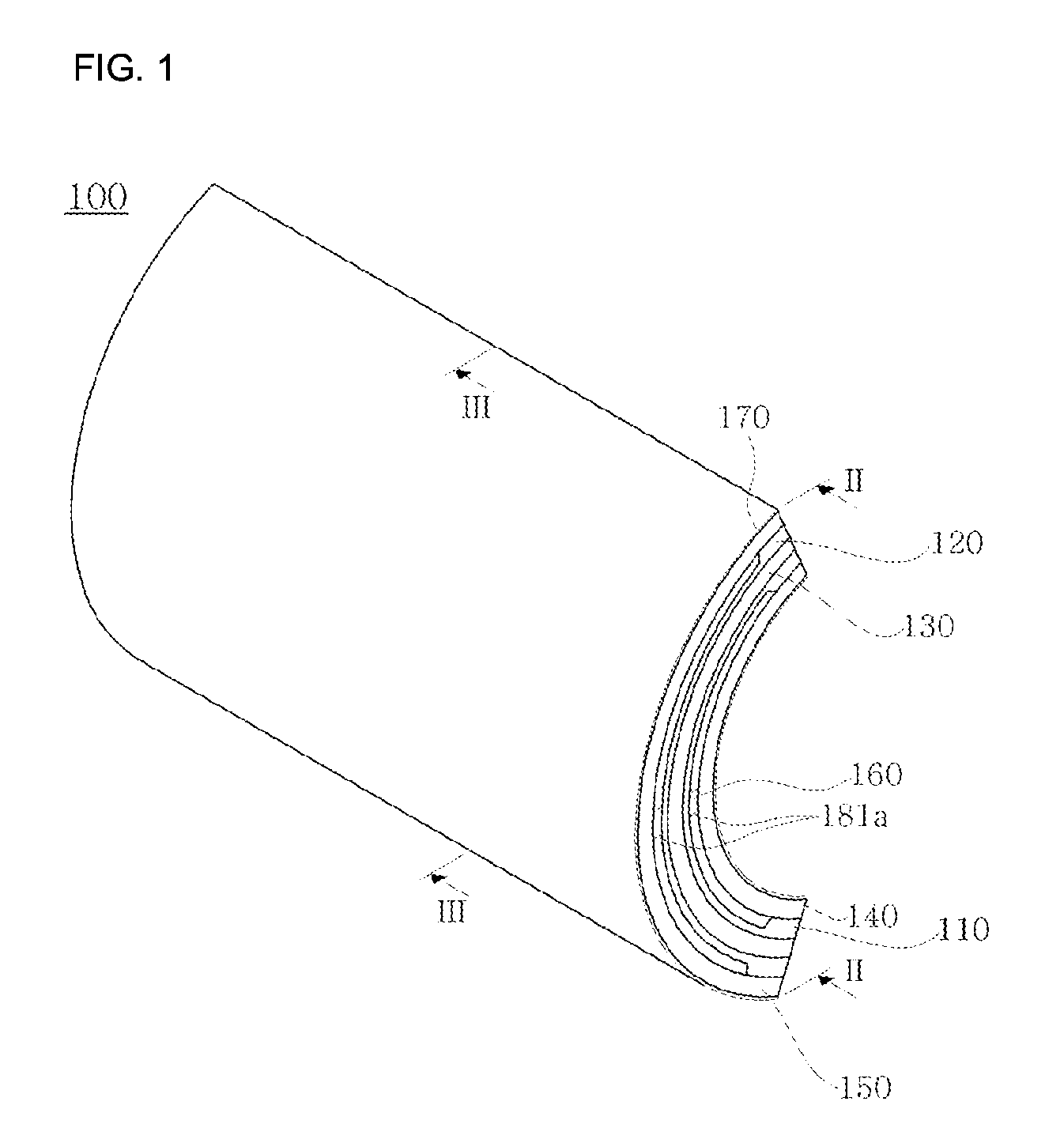
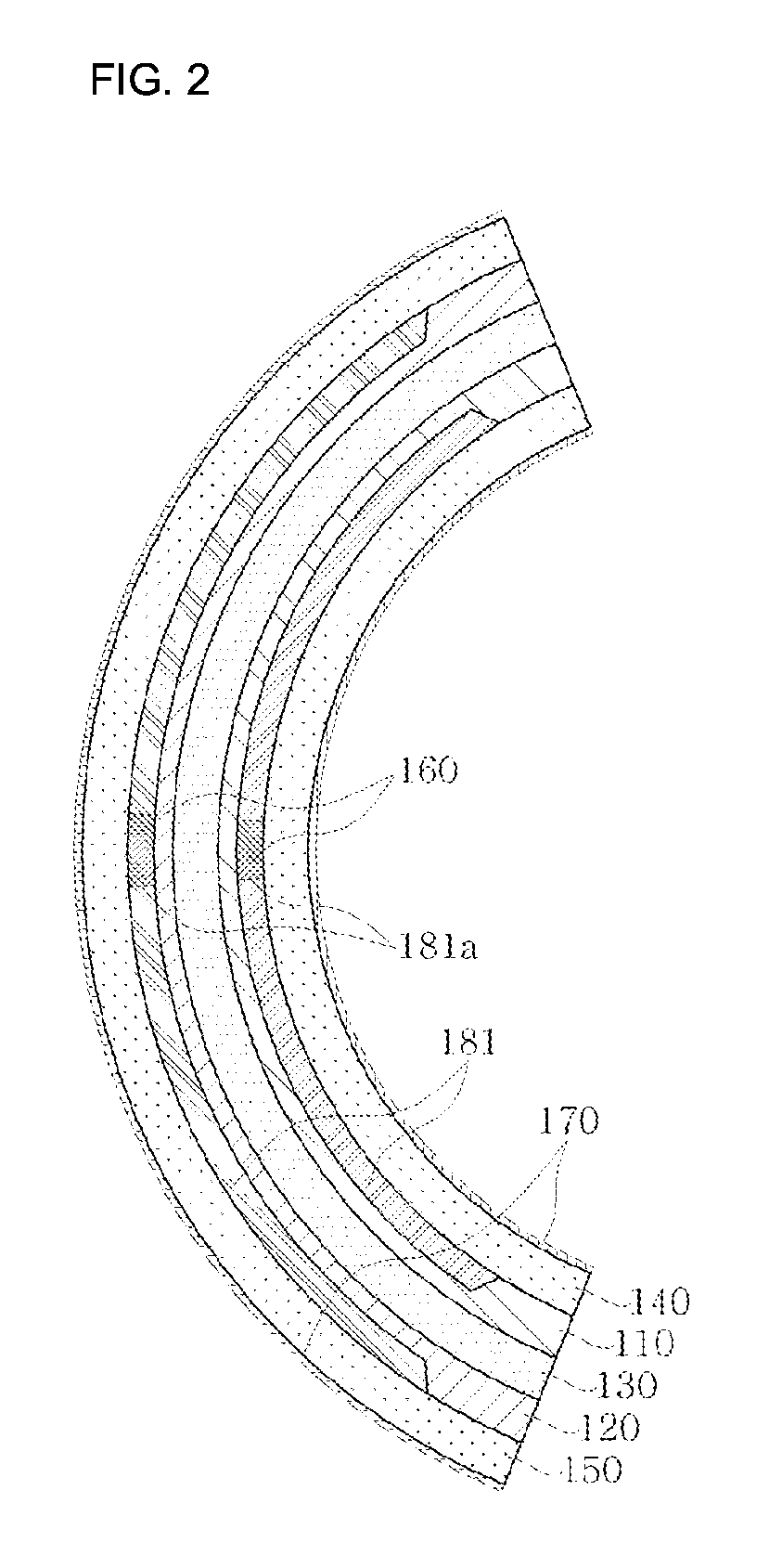
[0012]The present invention has been made in an effort to provide a curved-surface display panel fabrication method which can produces a display panel having a curved shape through a simple process using a conventional display panel having substrate and a curved-surface display panel which is fabricated by the method.

[0013]Furthermore, the present invention has also been made in an effort to provide a multi-image display device in which an image noise generated by the interference between the overlapped display panel can be prevented and the assembling process is simplified.

Technical Solution

[0014]In an exemplary embodiment of the present invention, a curved-surface display panel fabrication method for fabricating a curved-surface display panel having a desired curved shape using a flat display panel having a first substrate and a second substrate includes: paring partially outer surfaces of the first substrate and the second substrate so as to reduce thicknesses th...


PUM

PropertyMeasurementUnit
thicknessaaaaaaaaaa
thicknessaaaaaaaaaa
thicknessaaaaaaaaaa

Abstract

A curved-surface display panel fabrication method for fabricating a curved-surface display panel using a flat display panel having a first substrate and a second substrate includes: paring partially outer surfaces of the first substrate and the second substrate so as to reduce thicknesses thereof to a predetermined thickness; bending the pared flat display panel to a desired curved shape; attaching a first guide member which has a shape corresponding to the desired curved shape to the first substrate with a predetermined gap from the pared outer surface thereof and attaching a second guide member with has a shape corresponding to the desired curved shape to the second substrate with a predetermined gap from the pared outer surface thereof; and forming light transmitting reinforcing layers respectively in a space between the first guide member and the first substrate and a space between the second guide member and the second substrate.

Description

FIELD OF THE INVENTION[0001]The present invention relates to a curved-surface display panel fabrication method, a curved-surface display panel formed by the method, and a multi-image display device using the same.BACKGROUND ART[0002]Various display devices have been developed and are being used. A liquid crystal display device which realizes images using liquid crystal is widely used.[0003]Generally, a liquid crystal display (LCD) includes two display panels and a liquid crystal layer disposed therebetween and having a dielectric anisotropy. An electric filed is formed in the liquid crystal layer, and a transmittance of light passing the liquid crystal layer is regulated by regulating amplitude of the electric field so as to obtain a desired image. Such a liquid crystal display is representative one of a flat panel display (FPD), and TFT-LCD which uses thin film transistor (TFT) as a switching element is widely used.[0004]A plurality of display signal lines i.e., gate lines and data...

Claims


Application Information

Patent Timeline
Patent Type & Authority Patents(United States)
IPC IPC(8): H05K7/00H05K1/03B32B17/06G02F1/1333
CPCG02F1/1333B32B17/064G02F1/133305G02F2202/28G02F2001/133302B32B17/10G02F1/133302
Inventor KIM, YONG BEOMKIM, YANG RAE
Owner TOVIS
Why Eureka
Try Eureka