
Display device and method for driving same

a technology of display device and drive device, which is applied in the direction of semiconductor devices, instruments, electrical apparatus, etc., can solve the problems of increasing production costs, and achieve the effects of reducing power consumption, reducing the number of elements in the pixel circuit, and not reducing the aperture ratio

Active Publication Date: 2015-03-31
SHARP KK
View PDF36 Cites 2 Cited by
  • Summary
  • Abstract
  • Description
  • Claims
  • Application Information

AI Technical Summary

Benefits of technology

This patent text describes a technology for reducing the circuit size and power consumption of a display device by eliminating the need for signal lines and power control circuits. The technology also improves the accuracy and reliability of threshold detection and ensures a reliable initialization operation. Additionally, the technology can reduce variations in luminance and enhance moving picture performance by unlit pixel circuits. It also prevents differences in luminance at the screen center caused by the location of power lines. Furthermore, the technology reduces the circuit scale of the power control circuit by reducing the number of output buffers.

Problems solved by technology

In general, as the number of lines (particularly, control lines) connected to the pixel circuit increases, the circuit becomes more complicated, resulting in increased production cost.

Method used


Image

  • Display device and method for driving same
  • Display device and method for driving same
  • Display device and method for driving same

Examples


first embodiment

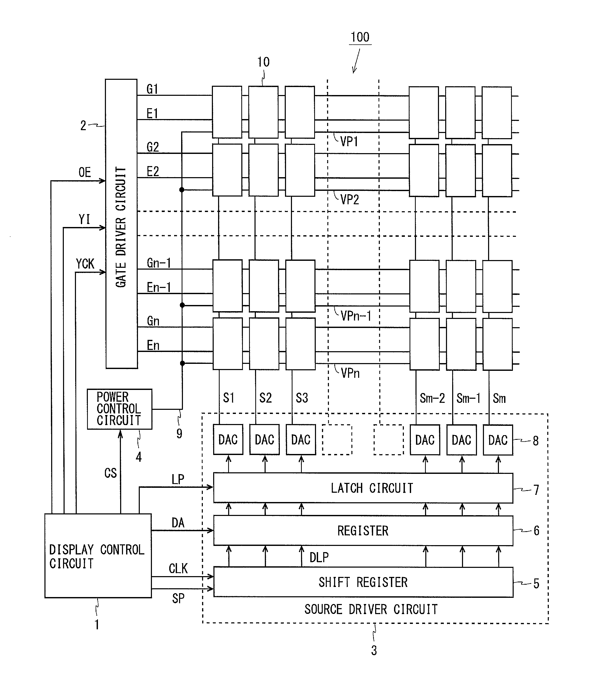
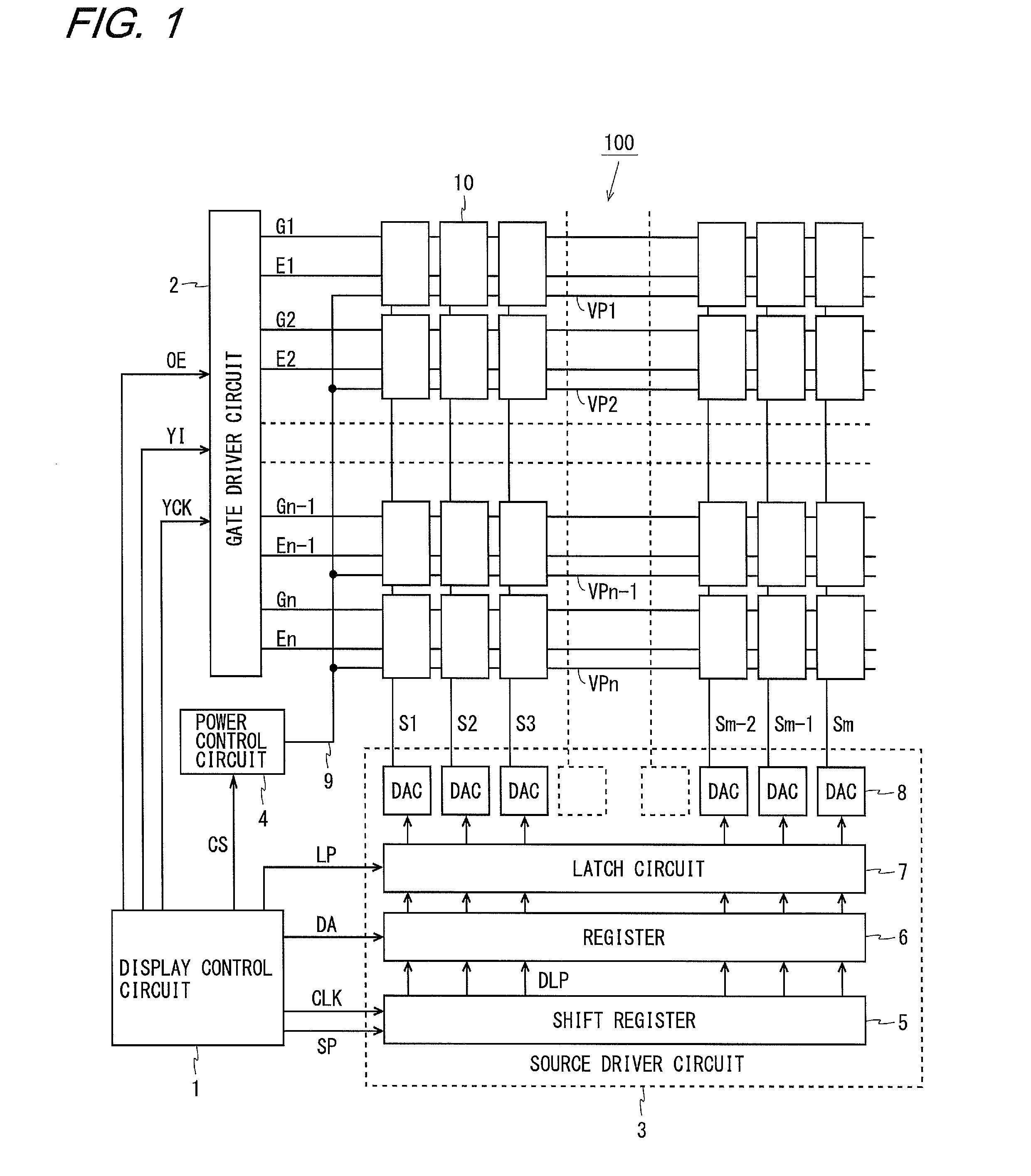
[0088]FIG. 1 is a block diagram illustrating the configuration of a display device according to a first embodiment of the present invention. The display device 100 shown in FIG. 1 is an organic EL display including a display control circuit 1, a gate driver circuit 2, a source driver circuit 3, a power control circuit 4, and (m×n) pixel circuits 10. Hereinafter, m and n are integers of 2 or more, i is an integer of 1 or more, and j is an integer of from 1 to m.

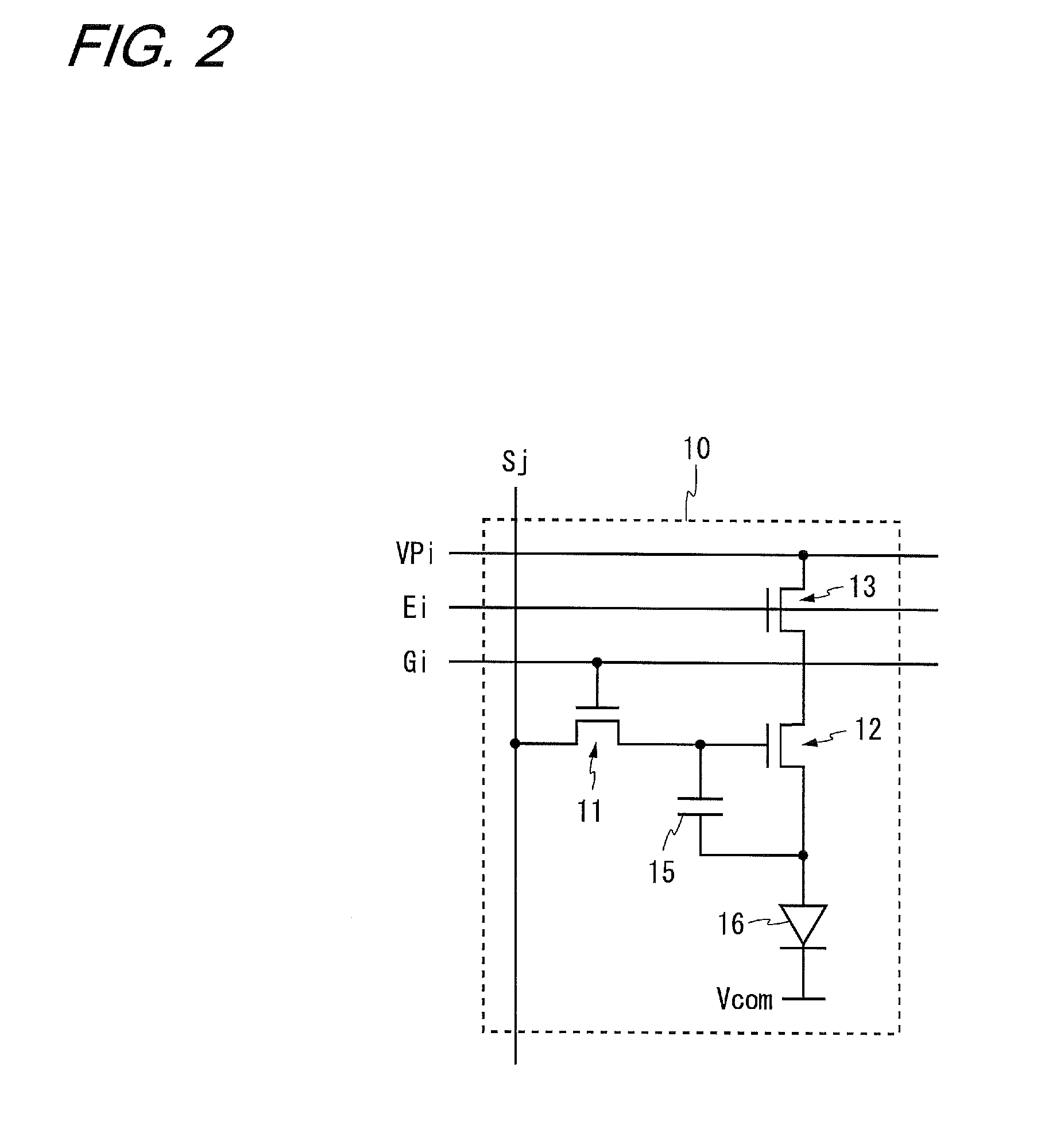
[0089]The display device 100 is provided with n parallel scanning signal lines Gi and m parallel data lines Sj perpendicular thereto. The (m×n) pixel circuits 10 are arranged in a matrix so as to correspond to intersections of the scanning signal lines Gi and the data lines Si. Moreover, n control lines Ei and n power lines VPi are provided parallel to the scanning signal lines Gi. In addition, there is provided a common power line 9, which is a current supply bus line for connecting the power control circuit 4 to the power li...

second embodiment

[0130]The configuration and operation of a display device according to a second embodiment of the present invention are approximately the same as those of the display device according to the first embodiment shown in FIG. 1, except for the connecting arrangement of the power lines and the operation of the pixel circuits, therefore, the same components are denoted by the same reference characters, and any descriptions thereof will be omitted. Hereinafter, features and operations characteristic of the second embodiment will be described.

[0131]FIG. 9 is a diagram illustrating the connecting arrangement of power lines VPi in the display device according to the second embodiment of the present invention. The display device is provided with two common power lines 121 and 122 for connecting a power control circuit 4b to the power lines VPi. The common power lines 121 and 122 are connected at one end to two output terminals, respectively, of the power control circuit 4b. Power lines VP1 to ...

third embodiment

[0136]The configuration and operation of a display device according to a third embodiment of the present invention are approximately the same as those of the display device according to the first embodiment shown in FIG. 1, except for the connecting arrangement of the power lines and the operation of the pixel circuits, therefore, the same components are denoted by the same reference characters, and any descriptions thereof will be omitted. Hereinafter, features and operations characteristic of the third embodiment will be described.

[0137]FIG. 11 is a diagram illustrating the connecting arrangement of power lines VPi in the display device according to the third embodiment of the present invention. The display device is provided with two common power lines 131 and 132 for connecting a power control circuit 4c to the power lines VPi. The common power lines 131 and 132 are connected at one end to two output terminals, respectively, of the power control circuit 4c. Power lines VP1, VP3,...


PUM


Abstract

A display device (100) includes a plurality of pixel circuits (10), a gate driver circuit (2) coupled to a plurality of scanning signal lines Gi and a plurality of control lines Ei, and a power control circuit (4) coupled to a plurality of power lines VPi via a common power line. The pixel circuits (10) each include an organic EL element, a plurality of TFTs, and a capacitor, and are controlled to collectively receive initialization potentials at the beginning of a frame through the power lines VPi, collectively perform threshold detection immediately thereafter, and then perform writing and light-emission operations. Thus, the aperture ratio of the pixel circuits (10) can be kept high, the power control circuit (4) typically has only one output buffer so that the circuit scale thereof is small, drive by potential is performed only once, so that power consumption is low, and threshold detection is performed only once, so that a sufficient amount of time can be ensured for a detection period.

Description

CROSS REFERENCE TO RELATED APPLICATIONS[0001]This is a U.S. National Phase patent application of PCT / JP2011 / 062581, filed Jun. 1, 2011, which claims priority to Japanese Patent Applications No. 2010-157625, filed Jul. 12, 2010, and No. 2010-202702, filed Sep. 10, 2010, each of which is hereby incorporated by reference in the present disclosure in its entirety.TECHNICAL FIELD[0002]The present invention relates to display devices, and more specifically, the invention relates to a display device, such as an organic EL display, which includes self-luminous elements driven by current, and a method for driving the same.BACKGROUND ART[0003]Organic EL (electroluminescent) displays are conventionally known as being thin display devices featuring high image quality and low power consumption. The organic EL display has a plurality of pixel circuits arranged in a matrix, each circuit including an organic EL element, which is a self-luminous element driven by current, and a drive transistor for ...

Claims


Application Information

Patent Timeline
Patent Type & Authority Patents(United States)
IPC IPC(8): G09G3/30G09G3/32H01L27/32
CPCG09G3/3258G09G3/3233H01L27/3276G09G2300/0819G09G2300/0842G09G2300/0861G09G2300/0866G09G2310/0205G09G2310/0218G09G2310/0256G09G2320/0252H10K59/131H10K59/121H10K59/1213H10K59/122H10K59/12
Inventor KISHI, NORITAKANOGUCHI, NOBORU
Owner SHARP KK
Learn More