Component of substrate processing apparatus and method for forming a film thereon

a substrate processing and film film technology, applied in the direction of water-setting substance layered products, transportation and packaging, coatings, etc., can solve the problems of increasing the size of the processing apparatus, and increasing the weight of the substrate processing apparatus, so as to reduce the risk of affecting the production process, and prevent the infiltration of cutting oil or the like into the film.

Active Publication Date: 2015-04-07
TOKYO ELECTRON LTD
View PDF9 Cites 2 Cited by
  • Summary
  • Abstract
  • Description
  • Claims
  • Application Information

AI Technical Summary

Benefits of technology

[0007]The present invention provides a component for a substrate processing apparatus and a film forming method, in which the generation of particles due to a damage of an alumite film can be reliably prevented.

Problems solved by technology

In recent years, the substrate processing apparatus has increased in size with the increase in the diameter of wafer and, therefore, the increase in the weight of the substrate processing apparatus has become an issue to be concerned about.
In the high power plasma processing, the temperature of a cooling plate rises, but a sealed alumite film generally has a low heat resistance.
For this reason, in the plasma processing, damages such as cracks develop in the alumite film formed on the cooling plate, and the alumite film is partially peeled off to generate particles.
Therefore, even though the alumite film is formed in accordance with the above-described alumite film forming method, the alumite film has an insufficient heat resistance, and the alumite film can be damaged, thereby generating particles.
If the hydration sealing is promoted, the heat resistance of the alumite film can be deteriorated, and thus the alumite film can be damaged to thereby generate particles.

Method used


Image

  • Component of substrate processing apparatus and method for forming a film thereon
  • Component of substrate processing apparatus and method for forming a film thereon
  • Component of substrate processing apparatus and method for forming a film thereon

Examples


Embodiment Construction

[0032]Hereinafter, an embodiment of the present invention will be described with reference to the accompanying drawings which form a part hereof.

[0033]First, a description will be made on a substrate processing apparatus to which a component of a substrate processing apparatus in accordance with the embodiment of the present invention is applied.

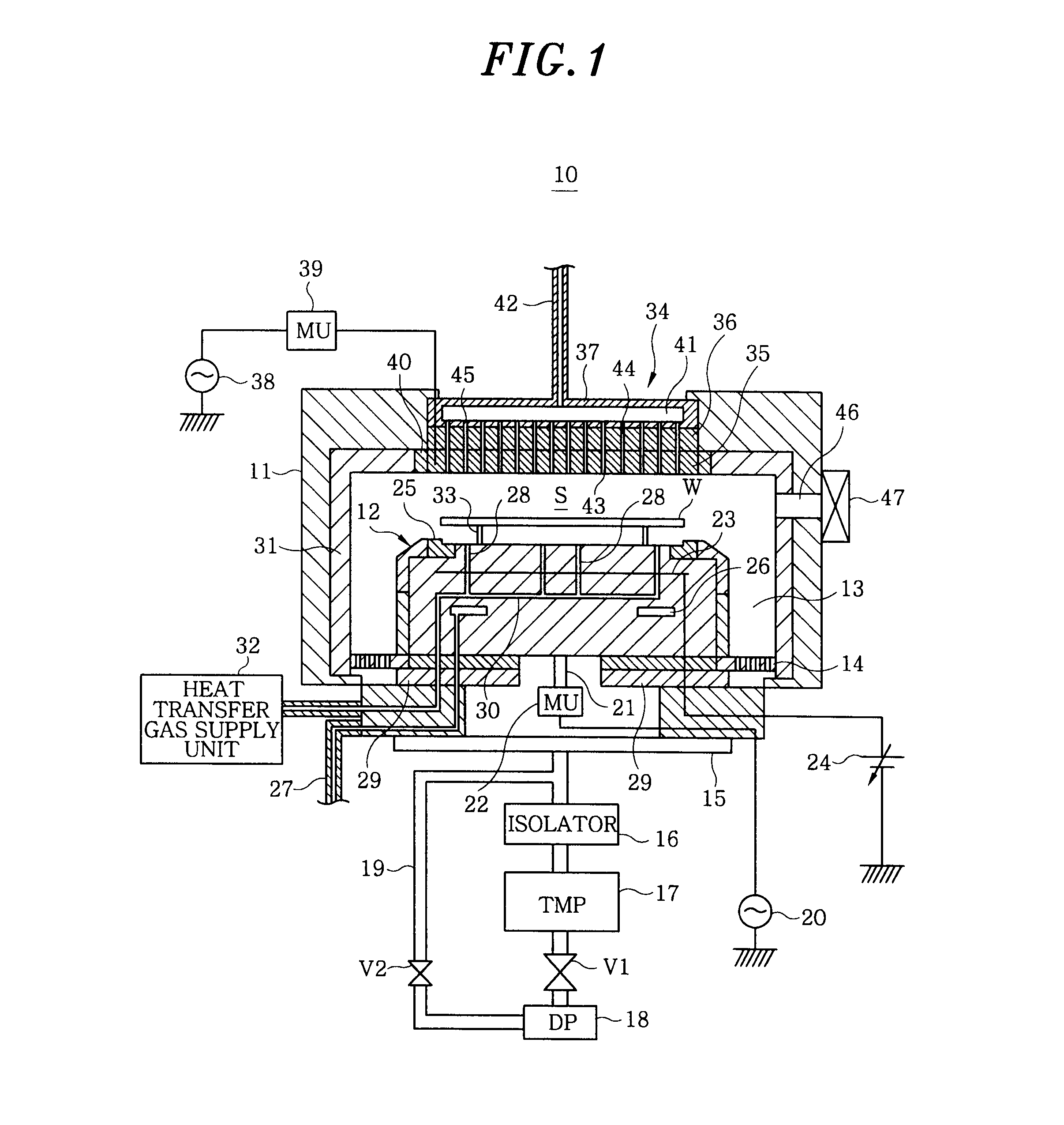
[0034]FIG. 1 is a cross-sectional view schematically showing a configuration of a substrate processing apparatus to which a component of a substrate processing apparatus in accordance with the embodiment of the present invention is applied. The substrate processing apparatus is configured to perform RIE (reactive ion etching) processing or ashing processing on a semiconductor wafer W as a substrate.

[0035]As shown in FIG. 1, a substrate processing apparatus 10 has a columnar chamber 11 which has a processing space S therein. In the chamber 11, a cylindrical susceptor 12 is disposed as a mounting table on which a semiconductor wafer (hereinaft...


PUM

PropertyMeasurementUnit
diameteraaaaaaaaaa
temperatureaaaaaaaaaa

Abstract

A component of a substrate processing apparatus that performs plasma processing on a substrate includes a base mainly formed of an aluminum alloy containing silicon. A film is formed on the surface of the base by an anodic oxidation process which includes connecting the component to an anode of a power supply and immersing the component in a solution mainly formed of an organic acid. The film is impregnated with ethyl silicate.

Description

FIELD OF THE INVENTION[0001]The present invention relates to a component of a substrate processing apparatus and a method for forming a film thereon, and more particularly to a component of a substrate processing apparatus that performs plasma processing on a substrate and a method for forming a film thereon.BACKGROUND OF THE INVENTION[0002]As substrate processing apparatuses for performing a predetermined processing on a wafer as a substrate, a film forming apparatus that performs film formation processing by CVD (chemical vapor deposition) or PVD (physical vapor deposition) and an etching apparatus that performs etching processing are known. In recent years, the substrate processing apparatus has increased in size with the increase in the diameter of wafer and, therefore, the increase in the weight of the substrate processing apparatus has become an issue to be concerned about. Thus, a lightweight aluminum member has been widely used as a material of components of the substrate pr...

Claims


Application Information

Patent Timeline
Patent Type & Authority Patents(United States)
IPC IPC(8): B32B3/02C25D5/00H01L21/31C25D11/00C25D11/24C25D21/02
CPCC25D21/02C25D11/246C25D11/005Y10T428/162Y10T428/218C25D11/02H01L21/00C25D11/24
Inventor MITSUHASHI, KOJI
Owner TOKYO ELECTRON LTD
Why Eureka
Try Eureka