Multilayer organic device

a multi-layer organic and device technology, applied in semiconductor devices, solid-state devices, electrical devices, etc., can solve the problems of high material wastage rate, inefficient single-layer organic devices for many applications, and difficulty in preparing multi-layer organic devices

Inactive Publication Date: 2015-06-09
THORN LIGHTING
View PDF16 Cites 116 Cited by
  • Summary
  • Abstract
  • Description
  • Claims
  • Application Information

AI Technical Summary

Benefits of technology

[0016]Accordingly, the present invention seeks to provide a multilayer organic device with minimal intermixing between layers using solutio

Problems solved by technology

However, different electron and hole mobility properties of the active material, non-ideal electron and hole injection from the electrodes and quenching by electrodes make single layer organic devices inefficient for many applications.
One limitation on manufacturing processes involving semiconducting polymers is the difficulties in preparing multilayer organic devices.
A challenge of forming such multilayer organic devices is one of building layers of the device without intermixing of layers or damaging existing layers during a layer depositing process.
A drawback of such vacuum deposition technique is that it requires both the use of expensive machinery and in addition leads to a high wastage rate of material.
However, the fabrication of multi-layer structures from solution faces severe challenges.
In depositing sequential layers, there is the problem that the solvents might re-dissolve previously deposited layers, resulting potentially in intermixing of layers or damaging of existing layers during a layer depositing process.
It might also cause process irreproducibility or reduced efficiency of the resulting devices.
As a matter of fact, only few solution proce

Method used


Image

  • Multilayer organic device
  • Multilayer organic device
  • Multilayer organic device

Examples


example 1

Bilayer Hole Injection Layer Device

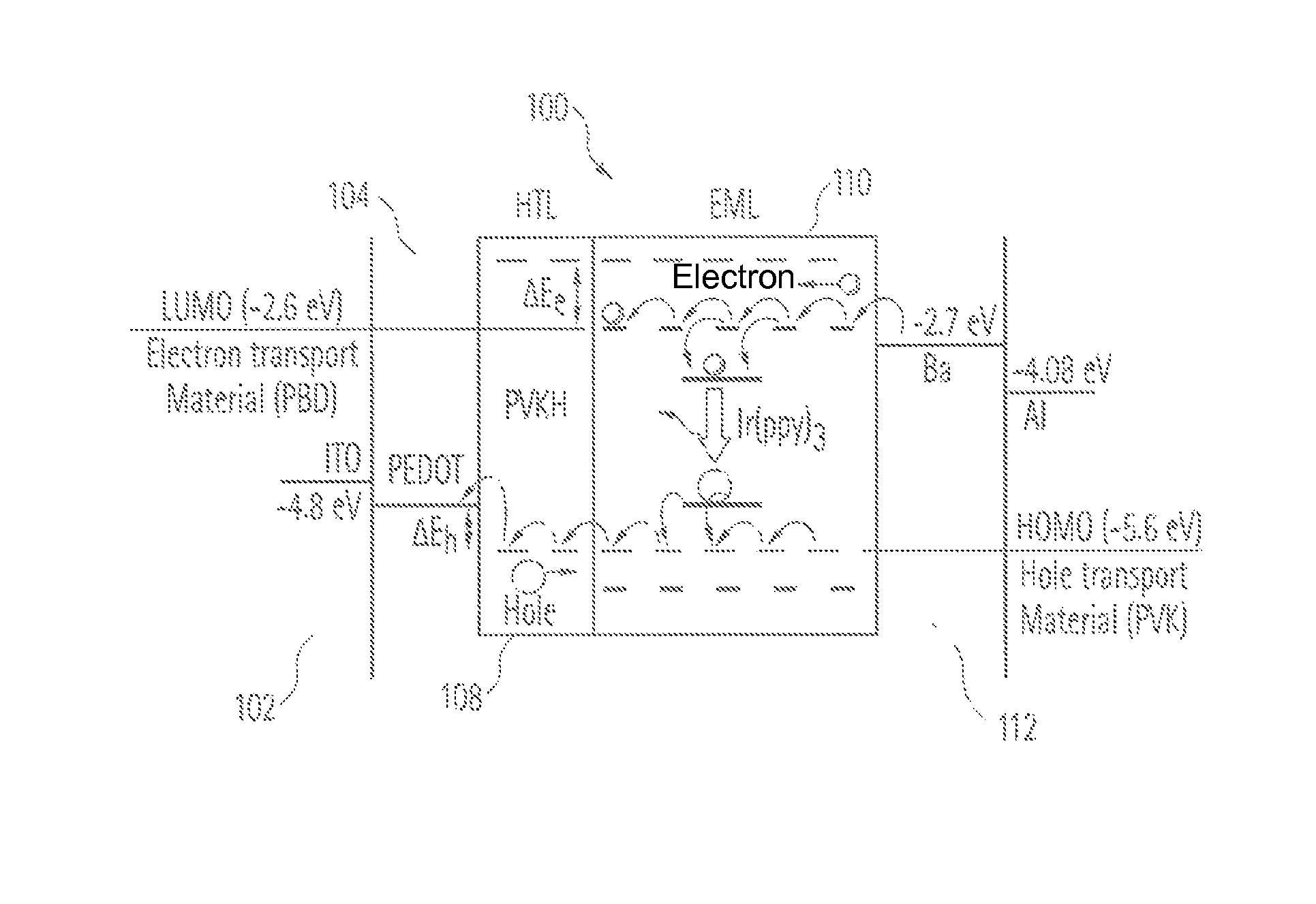
[0085]Referring to the first example shown in FIG. 6, the device 100 comprises at first a glass substrate (not shown in FIG. 6) supporting a patterned anode made of indium tin oxide (ITO) 102. A hole injection layer 104 comprised of a conducting polymer poly(3,4-ethylenedioxy thiophene) / poly(styrenesulfonate) (PEDOT:PSS) 104 is deposited over the indium tin oxide 102. Further, over the PEDOT:PSS is deposited a layer of high average molecular weight poly (vinyl carbozole) (PVKH) 108 acting as a hole transport layer (HTL). Subsequent emission layer (EML) 110 comprises low molecular weight poly (vinyl carbozole) doped with an phosphorescent emitter species Ir(ppy)3. A Barium Aluminium cathode 112 is deposited over the emission layer 110 using evaporation techniques known in the art.

[0086]The device fabrication is described in detail the experimental section below. The device architecture and the schematic energy level diagrams for materials used in th...

example 2

Bi-Layers White Light Emitting Device

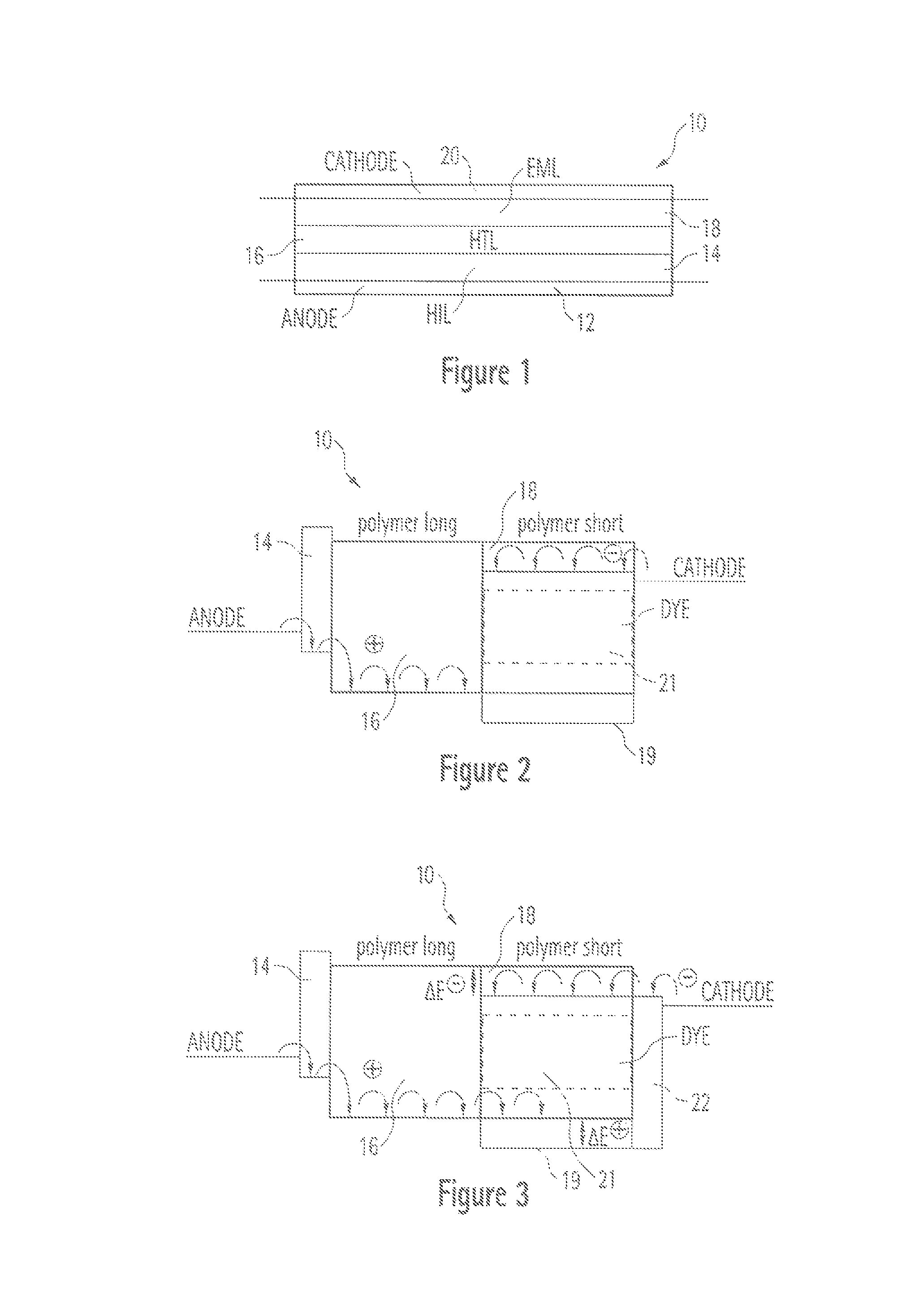
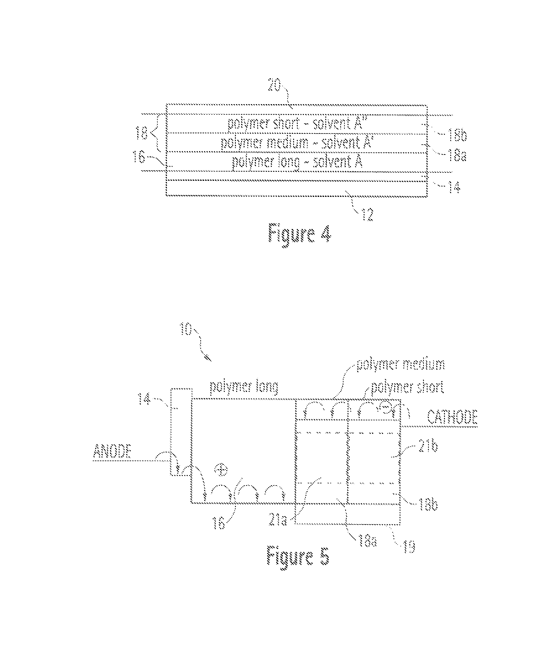
[0107]The structure of the second specific example of a multilayer organic device is shown in FIGS. 12 to 14. This embodiment forms a so called multicolours organic LED to generate white light for back-lighting or general lighting applications.

[0108]The white light generated in this embodiment comprises only two nonsaturated colours (blue-green and yellow emitters) instead of three saturated colours (blue, green and red). The device structure comprises a similar layer structure order to that described in Example 1. The hole transport layer (HTL) in the first example has now been used to form a yellow emissive layer (EML1) which comprises a mixture of host material (PVKH), electron transport material and yellow emissive dopant spin coated from chlorobenzen solution. The host material (PVKH) is preferably mixed with low concentration electron transport material <20% w / w, to avoid losing PVKH resistance to the second layer solvent. The second layer ...


PUM

PropertyMeasurementUnit
Thicknessaaaaaaaaaa
Lengthaaaaaaaaaa
Electric chargeaaaaaaaaaa

Abstract

In a multilayer organic device (10) comprising a substrate bearing an anode (12) and a cathode (20), wherein located between the anode (12) and the cathode (20) is at least a first layer (16) comprising a first organic semiconductor material; and a second layer (18) over the first layer (16) comprising a second organic semiconductor material; the first organic semiconductor material is a polymer and the second organic material is a polymer or an oligomer, the average molecular weight of the first organic semiconductor material being higher than the average molecular weight of the second organic semiconductor material.

Description

BACKGROUND OF THE INVENTION[0001]The present invention relates, in general, to a multilayer organic device and a method of fabricating such a device. More particularly, such a multilayer organic device can be an organic electroluminescent device comprising a polymeric light emitting diode (PLED) or a photoresponsive device such as a solar cell forming a polymeric organic photovoltaic (OPV) device.[0002]Semiconducting polymers make remarkably effective substitutes for conventional inorganic semiconductors in a range of optoelectronic devices. Such devices can include light emitting diodes (LEDs), photovoltaic (PV) diodes, field effect transistors (FETs), and lasers. Conjugated polymers offer considerable material advantages over inorganic semiconductors including chemically tunable optoelectronic properties and low-temperature, solution-based processing suitable for printed electronics.[0003]A single layer organic device comprises a pair of electrodes and an active material generally...

Claims


Application Information

Patent Timeline
IPC IPC(8): H01L51/30H01L51/00H01L51/50
CPCH01L51/0042H01L51/0003H01L51/0035H01L51/0085H01L51/5016H10K71/12H10K85/146H10K85/111H10K85/342H10K50/11H10K2101/10H10K10/00
Inventor MONKMAN, ANDREWAL-ATTAR, HAMEED
Owner THORN LIGHTING
Why Eureka
Try Eureka