Electro-optical module

a technology of electrooptical modules and optical modules, applied in semiconductor lasers, semiconductor/solid-state device details, lasers, etc., can solve problems such as signal loss and electromagnetic interference, and achieve the effects of reducing the size of the electrooptical module, reducing the signal transmission distance, and limited loop length and heigh

Active Publication Date: 2015-06-16
SILICONWARE PRECISION IND CO LTD
View PDF8 Cites 6 Cited by
  • Summary
  • Abstract
  • Description
  • Claims
  • Application Information

AI Technical Summary

Benefits of technology

[0023]By electrically connecting the electro-optical element to the interposer in a flip-chip manner and further electrically connecting the electro-optical element to the substrate through the interposer, the invention reduces the size of the electro-optical module, dispenses with the conventional bonding wires that are limited in loop length and height, and reduces the signal transmission distance. Therefore, the invention reduces signal losses during high frequency signal transmission. As such, the electro-optical module is applicable to high frequency signal transmission.
[0024]Further, by fixing the transparent plate to the substrate through the support members, the invention improves the accuracy of alignment between the lens portion of the transparent plate and the electro-optical element on the substrate. Furthermore, the support members made of metal provide an EMI shielding effect so as to improve the quality of high frequency communication.
[0025]Moreover, by embedding a heat sink in the substrate and disposing the electro-optical element and the semiconductor element on the heat sink, the invention achieves a preferred thermal dissipation effect.
[0026]Therefore, the invention overcomes the conventional disadvantage of signal losses caused by wire bonding, improves the accuracy of alignment, and achieves preferred EMI shielding and heat dissipating effects.

Problems solved by technology

However, such a wire bonding method can easily result in signal losses and electromagnetic interferences during high frequency signal transmission.

Method used


Image

  • Electro-optical module
  • Electro-optical module
  • Electro-optical module

Examples


Embodiment Construction

[0033]The following illustrative embodiments are provided to illustrate the disclosure of the present invention, these and other advantages and effects can be apparent to those in the art after reading this specification.

[0034]It should be noted that all the drawings are not intended to limit the present invention. Various modifications and variations can be made without departing from the spirit of the present invention. Further, terms such as “top”, “bottom”, “first”, “second” etc. are merely for illustrative purposes and should not be construed to limit the scope of the present invention.

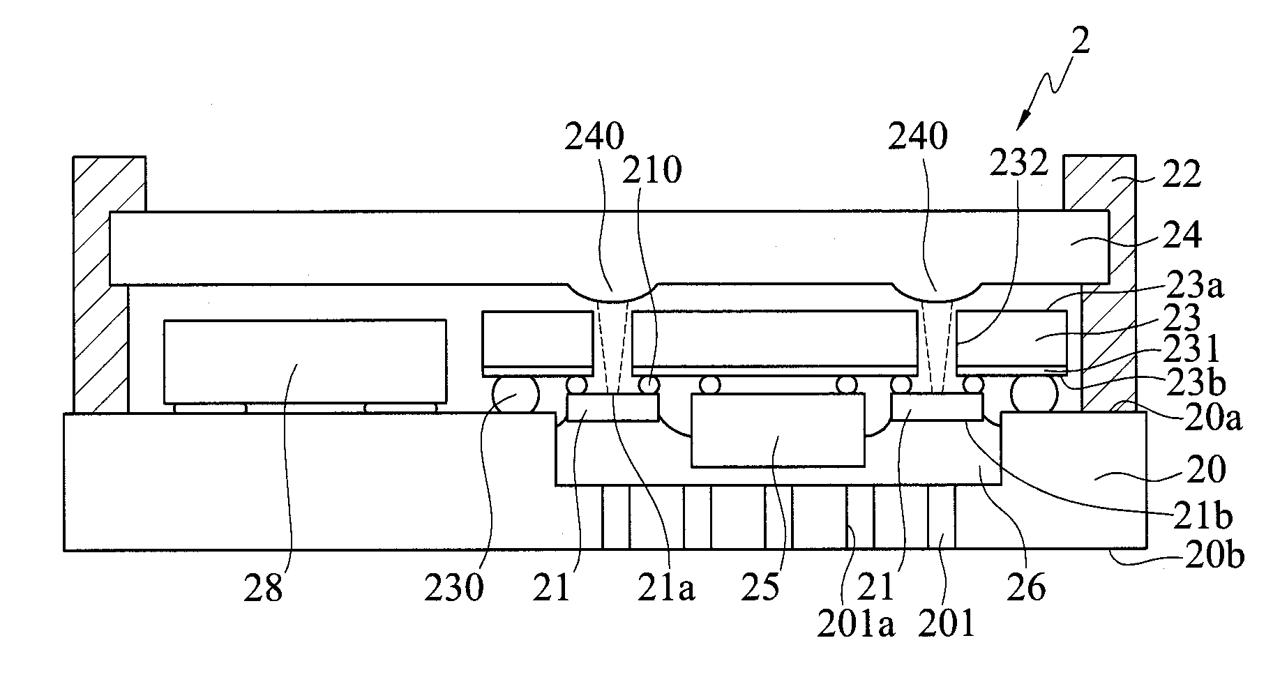
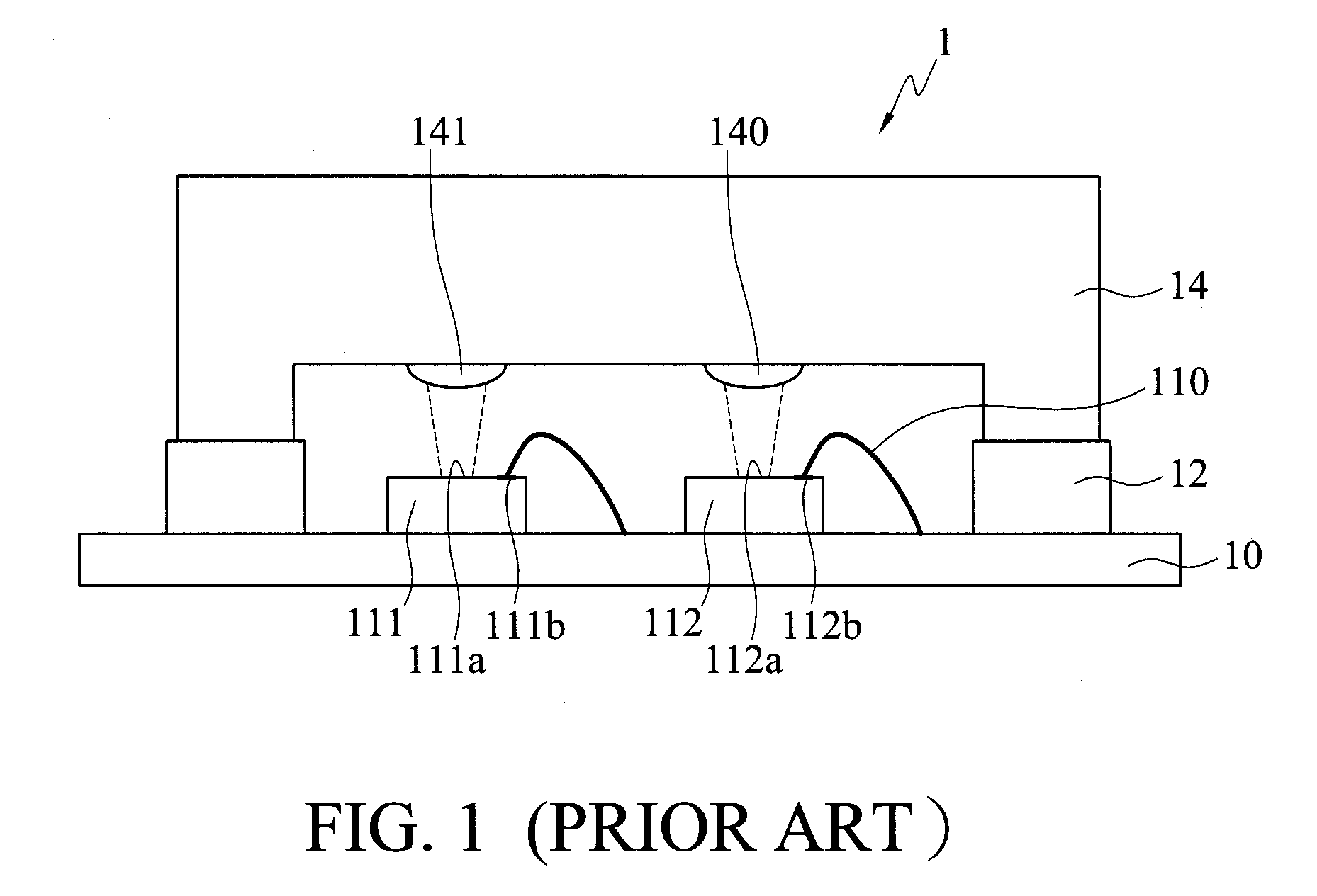
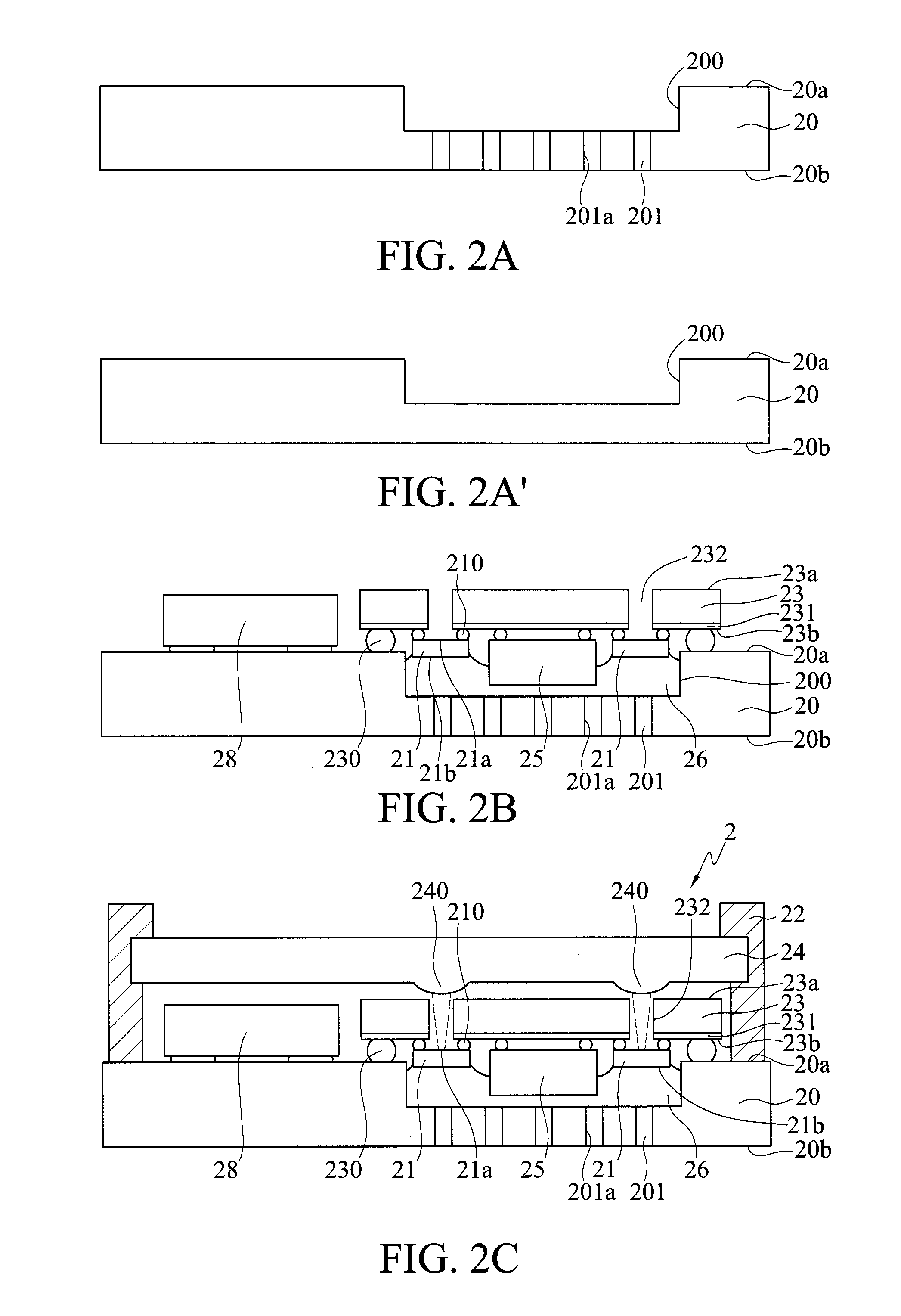
[0035]FIGS. 2A to 2C are schematic cross-sectional views illustrating an electro-optical module 2 and a fabrication method thereof according to an embodiment of the present invention. Therein, FIG. 2A′ illustrates another embodiment of FIG. 2A.

[0036]Referring to FIG. 2A, a substrate 20 having a first surface 20a with a groove 200 and a second surface 20b opposite the first surface 20a is provided...


PUM


Abstract

An electro-optical module is provided, which includes: a substrate having a first surface with a groove and an opposite second surface; a plurality of support members disposed on the first surface of the substrate; at least an electro-optical element having opposite active and non-active surfaces and disposed in the groove of the substrate via the non-active surface thereof; an interposer disposed on the first surface of the substrate and the electro-optical element for electrically connecting the electro-optical element to the substrate, wherein the interposer has a through hole corresponding in position to the active surface of the electro-optical element; and a transparent plate disposed over the first surface of the substrate and the interposer through the support members and having a lens portion corresponding in position to the through hole of the interposer, thereby reducing signal losses, improving alignment precision, and achieving preferred thermal dissipation and EMI shielding effects.

Description

CROSS-REFERENCES TO RELATED APPLICATIONS[0001]This application claims under 35 U.S.C. §119(a) the benefit of Taiwanese Application No. 102100202, filed Jan. 4, 2013, the entire contents of which is incorporated herein by reference.BACKGROUND OF THE INVENTION[0002]1. Field of the Invention[0003]The present invention relates to anti-electromagnetic interference (anti-EMI) electro-optical modules, and more particularly, to an electro-optical module in which an electro-optical element is electrically connected to an interposer in a flip-chip manner to reduce the size of the electro-optical module.[0004]2. Description of Related Art[0005]Along with the development of semiconductor fabrication technologies, a chip can be integrated with not only electronic elements but also biological, electro-optical, mechanical, electrical or magnetic elements. For example, a laser diode chip is integrated with both electro-optical and electrical functions. There are three types of laser diodes: fabry-p...

Claims


Application Information

Patent Timeline
Patent Type & Authority Patents(United States)
IPC IPC(8): H01L27/15H01L29/26H01S5/022H01L25/00H01L31/12H01L33/00H01S5/062H01S5/024H01S5/42
CPCH01L25/00H01S5/02252H01S5/02288H01S5/0226H01S5/02276H01S5/02469H01S5/06226H01S5/423H01L2224/48091H01L2924/00014H01L23/552H01L25/04H01S5/0236H01S5/02326H01S5/02345H01S5/02253
Inventor SHIH, CHIH-YUANPENG, SHIH-LIANGHUANG, JUNG-PINKU, CHIN-YUCHEN, HSIEN-WEN
Owner SILICONWARE PRECISION IND CO LTD
Why Eureka
Try Eureka